
Key Words: Silicon Wafer Dicing PCB Depaneling Glass Cutting
Home > News > Industry News
【Description】:
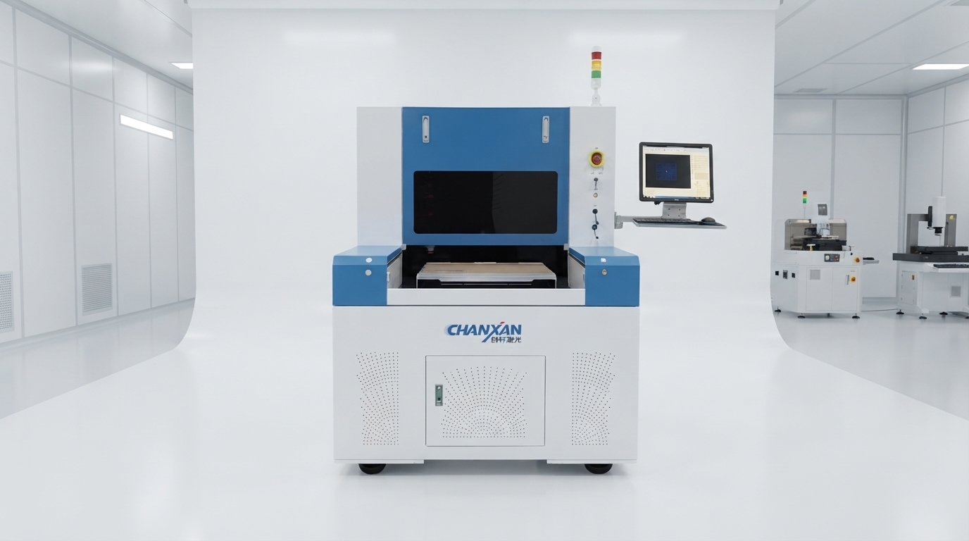
Chanxan CW-6050PZ picosecond laser performs cold ablation cutting on boron nitride sheet, avoiding delamination and microcracks for semiconductor thermal ceramic. Free sample cutting service available.
Boron nitride sheet (h‑BN) is a critical layered thermal‑conductive ceramic widely used for semiconductor gaskets, IGBT heat‑sink components and 5G RF thermal spreaders. Traditional nanosecond laser or mechanical dicing easily triggers inter‑layer delamination, micro‑cracks and edge carbonization. These defects will degrade thermal conductivity and dielectric performance, resulting in high scrap rates for thermal‑interface‑material manufacturers and semiconductor component factories.
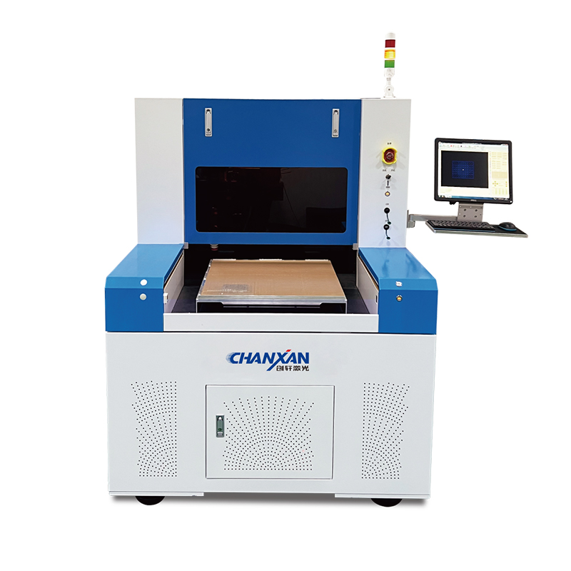
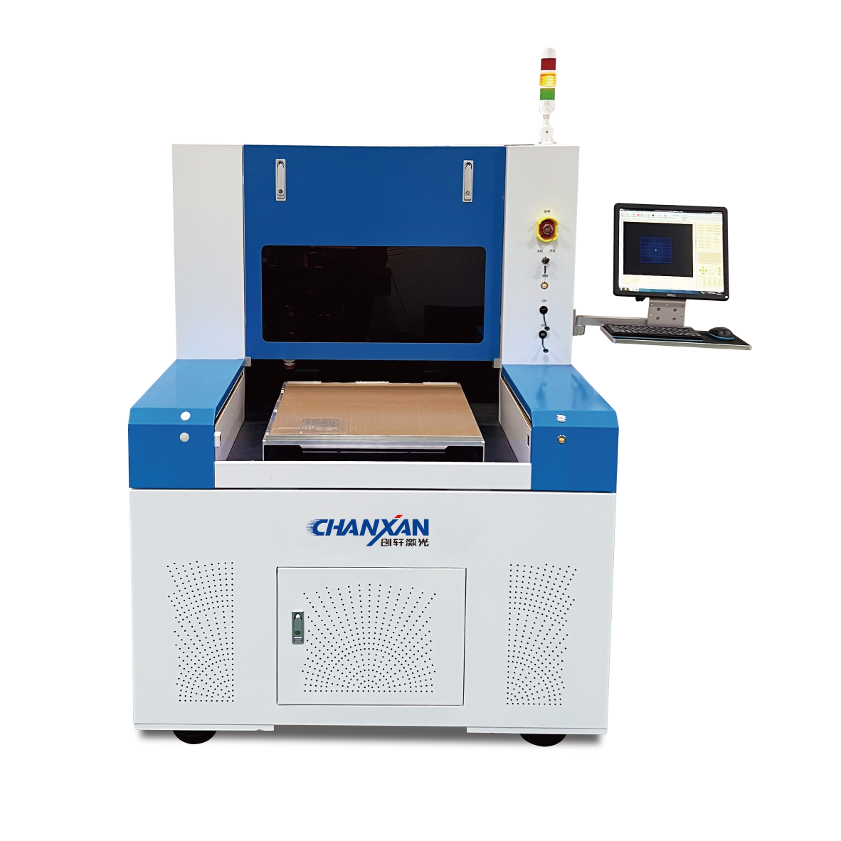
Chanxan launches optimized picosecond laser cutting machine CW‑6050PZ, specially developed for boron nitride sheet and brittle advanced ceramic processing. With ultrashort‑pulse cold ablation mechanism, it removes material by breaking molecular bonds instead of thermal melting. It effectively avoids thermal shock damage to layered ceramics, suitable for prototype R&D verification and large‑volume industrial mass‑production.
This ultrafast laser system solves typical pain‑points of boron nitride ceramic manufacturing via industrial‑grade hardware configuration:
‑ True cold‑ablation processing, minimal HAZ, eliminates delamination and carbonization on layered boron nitride sheet.
‑ High‑resolution coaxial CCD vision alignment, supports complex custom outlines without expensive custom moulds.
‑ Class‑00 granite base plus linear‑motor drive, guarantees long‑term stable micron‑level positioning accuracy.
Core technical parameters:
‑ Laser Source: Industrial Picosecond UV/Green ultrafast laser
‑ Positioning Repeatability: ±1 μm
‑ Max processing thickness: ≤3 mm for boron nitride & advanced ceramics
‑ Max processing speed: ≤3000 mm/s
For full technical specification sheet and configurable options, please visit our product detail page.
This CW‑6050PZ picosecond laser system serves semiconductor component manufacturers, thermal‑interface‑material factories and precision die‑cut service providers. Main target materials cover boron nitride sheet, AlN substrate, PI film, FPC and other brittle thin‑film electronics materials. Widely deployed for semiconductor packaging, automotive power electronics, 5G RF components and aerospace thermal‑management projects.
Yes. It supports aluminum nitride (AlN), alumina ceramics, PI, FPC and a variety of thin brittle electronic substrate materials for semiconductor manufacturing.
No physical mould required. Only CAD drawings are needed for custom‑shape cutting, greatly shortening prototype sample‑development and verification cycles.
Send boron‑nitride sheet samples and CAD drawings for feasibility assessment, get technical proposal and formal quotation.
Contact Us| Free solution
Previous: Picosecond Cold‑Ablation Cutting Improves Solder Preform Yield for Semiconductor Packaging
Next: UV Nanosecond Laser Cutting Machine for High-Precision Graphene Thermal Pad Processing