Key Words: Silicon Wafer Dicing PCB Depaneling Glass Cutting
Home > Products > Laser Micromachining Systems


Burr-Free Cold Processing for Thermal Conductive Ceramic Films
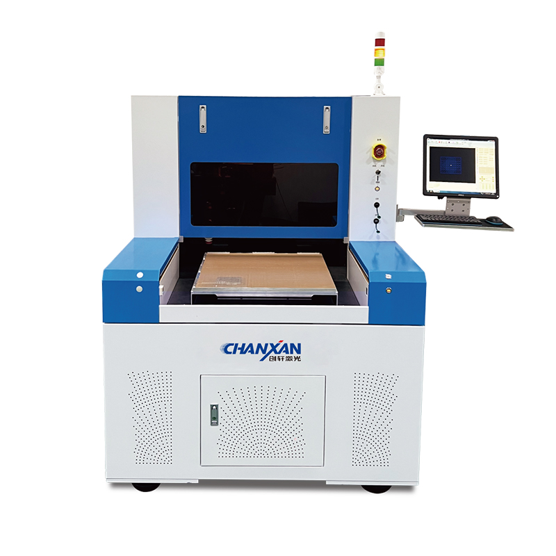
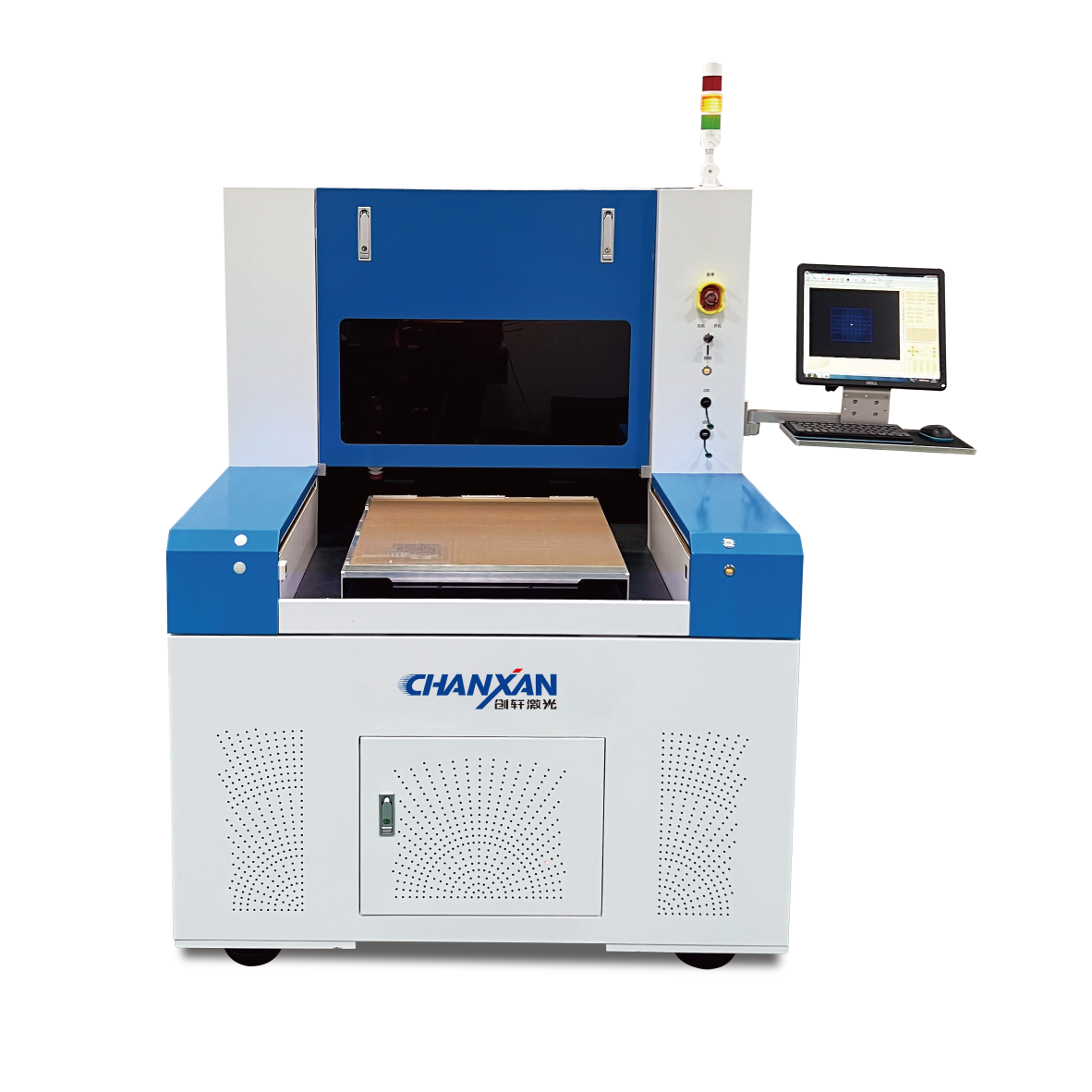
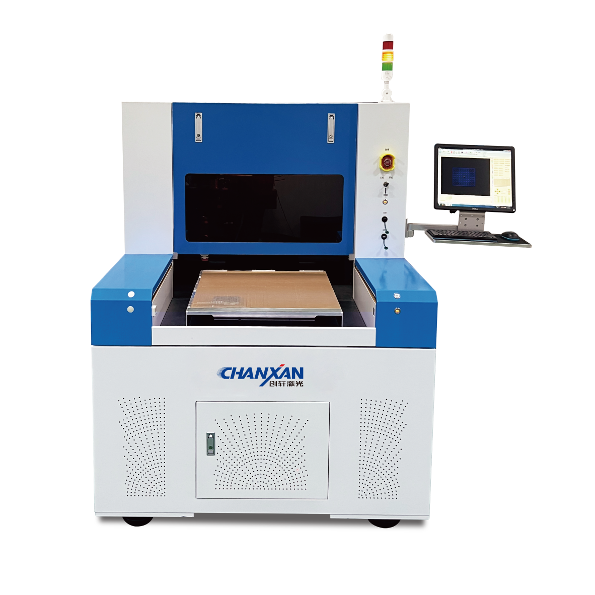
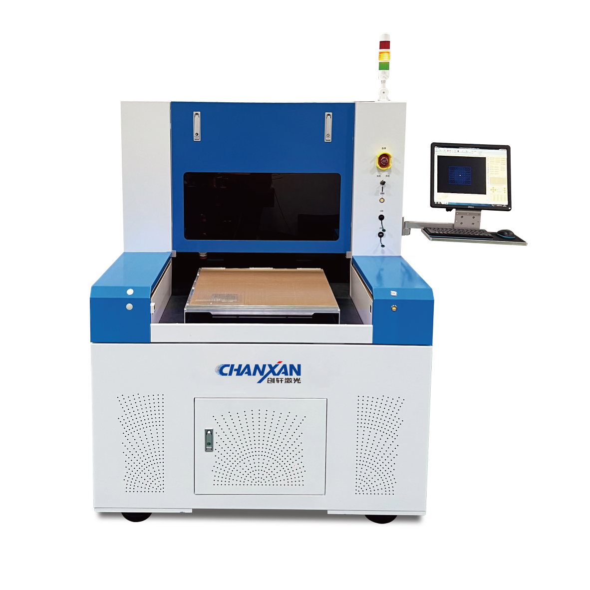
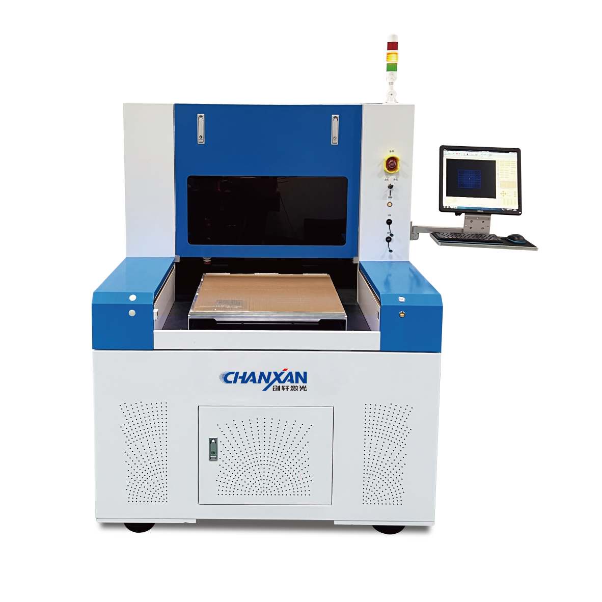
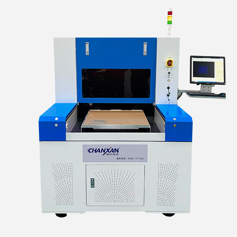
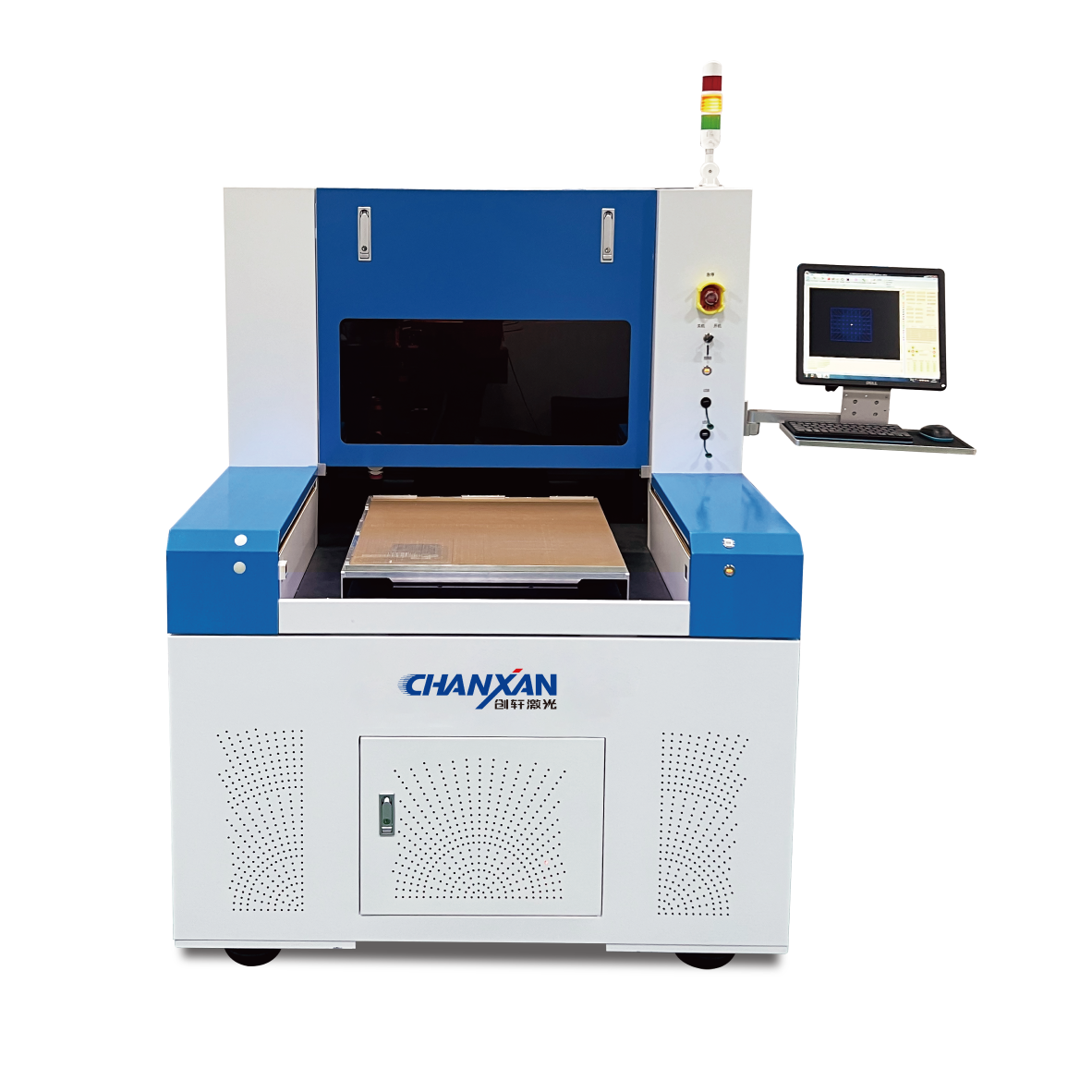
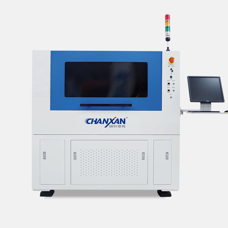
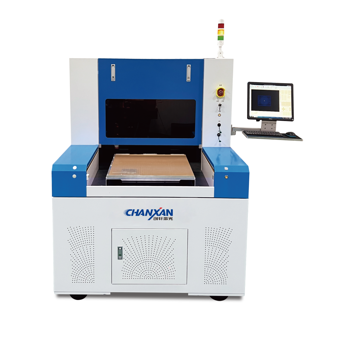
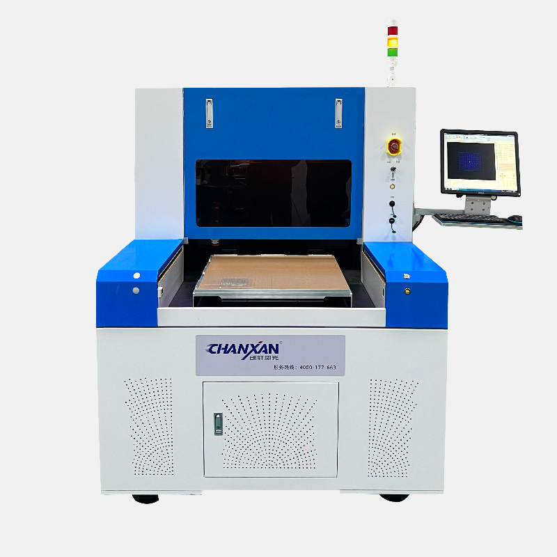
Our Precision Picosecond Laser Cutting Machine specializes in boron nitride sheet cold processing. The ultra-short picosecond laser delivers minimal HAZ, burr-free and carbonization-free cutting for thermal conductive ceramic films. It adopts marble linear motor platform and high-precision CCD alignment system, ideal for semiconductor, 3C electronics, automotive and aerospace industries. Compatible with Boron Nitride Sheet, PI Film, FPC, PCB and other non-metal flexible films. CE certified, with 12-month warranty and lifetime remote technical support.
Picosecond cold laser cutting for boron nitride sheet, minimal HAZ, burr‑free cutting.
Ultrafast cold ablation physics applied directly to anisotropic hexagonal boron nitride ceramic substrates.
Boron nitride cleaves easily with standard nanosecond and fiber lasers.
✕ Severe inter‑layer delamination from intense thermal shock waves.
✕ Heavy recast layers and brittle micro‑cracks along the cleavage plane.
✕ Wafer scrap rates exceeding 35% on high‑density RF gaskets.
Ultrafast picosecond cold laser ablation directly vaporizes covalent bonds.
✔ Sub‑10 picosecond pulses eliminate heat transfer to surrounding lattices.
✔ Pure cold ionization delivers pristine burr‑free vertical sidewalls.
✔ Yield rate achieved at 99.8% on micro‑aperture heat sink arrays.
Monolithic natural black granite eliminates thermal drift and absorbs micro‑vibrations during dynamic high‑speed pathing.
Ironless magnetic linear drive pairs with Renishaw optical scales achieving ±1.0 μm absolute position accuracy.
Constant 90‑degree incident beam perpendicularity ensures perfectly vertical edge profiles without taper across the full field.
Engineered specifically for micron‑tolerance cleanroom semiconductor substrate fabrication.
<10 ps ultrashort pulse eliminates heat‑affected zone (<2.0 μm) on boron nitride.
Sub‑micron focused spot yields clean vertical kerfs without melting or edge burning.
20 MP automatic optical alignment compensates workpiece orientation and warp.
Monolithic natural granite base ensures vibration‑free dynamic contouring.
Constant thermal control preserves beam energy stability during 24/7 industrial runs.
Complete laser safety interlocks and integrated cleanroom HEPA exhaust interface.
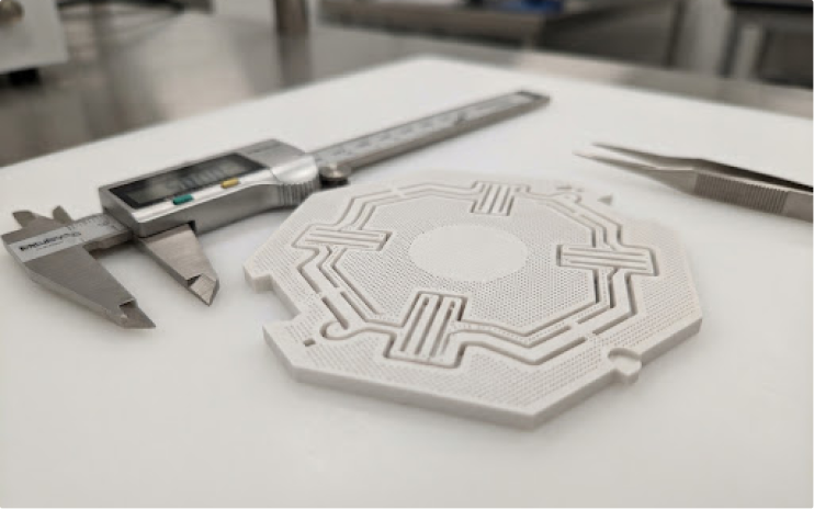
100% burr‑free edge, zero inter‑layer delamination, Ra < 0.4 μm mirror cut.
• Thermal Conductivity: > 65 W/(m·K) uncompromised
• Dielectric Breakdown: > 35 kV/mm intact
• Hole Array Pitch: Down to 50 μm center-to-center
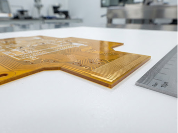
Ultra‑clean contouring without edge charring or thermal deformation on flexible circuits.
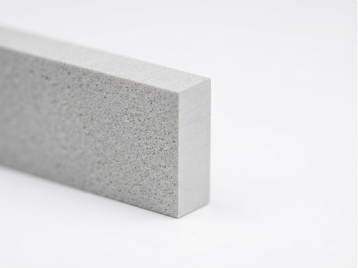
Micro‑crack free dicing for high‑power semiconductor packaging modules.
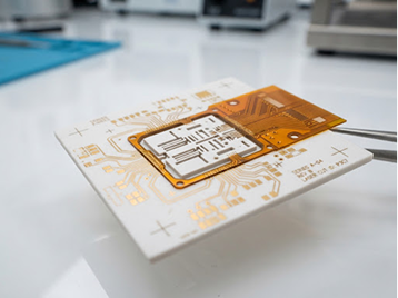
Precise aperture drilling and intricate outer perimeter geometry slicing.
| System Parameter | Engineering Specification |
|---|---|
| Laser Source & Wavelength | Industrial Picosecond UV (355nm) / Green (532nm) Solid‑State Optic Engine |
| Pulse Duration | < 10 ps (Athermal Non‑Linear Cold Ablation Regime) |
| Effective Working Area | 500 × 500 mm (Customizable up to 800 × 800 mm upon Cleanroom RFQ) |
| Positioning & Repeatability | ± 1.5 μm (Full Stage Stroke) / ± 1.0 μm (Renishaw Optical Feedback) |
| Processing Thickness | 0.05 mm – 3.0 mm (h‑BN / AlN / Alumina / Borosilicate Thin Films) |
| Motion Foundation & Drives | Dual‑Drive Ironless Magnetic Linear Motors + Monolithic Class 00 Granite Bed |
| Optical Spot Diameter | ≤ 15 μm (High‑Resolution Coaxial Telecentric F‑Theta Lens) |
| Safety & Cleanroom Compatibility | CE Certified, FDA/CDRH Laser Class 1 Interlocked, Exhaust HEPA Port Equipped |
SEM 1500x Inspection: Complete elimination of thermal micro‑cracking and zero edge delamination on layered h‑BN sheets.
Inter‑layer crystal plane preserved
Negligible thermal radiation impact
Zero conductive carbon residue
Comprehensive maintenance coverage on laser source and core optical modules with express replacement.
Factory optical engineers connect via secure encrypted telemetry within 2 hours of inquiry.
100% cutting validation performed on your supplied material before machine dispatch.
Shock‑absorbing, moisture‑sealed packaging certified for intercontinental air and sea freight.
Picosecond pulses vaporize material before heat conducts, preventing brittle layer fracture and carbonization.
Kerf width is down to ≤15 μm with maximum thickness up to 3.0 mm depending on ceramic density.
Yes. Send your CAD drawing (.DXF/.DWG) and sample material for free cut analysis within 48 hours.
Fully compliant with CE and FDA/CDRH Class 1 standards, suitable for ISO Class 1000 cleanrooms.
Get free sample-cut evaluation, quotation and technical support for CW-6050PZ picosecond laser machine.
Go To Contact Us Page →Submit your material requirements & CAD drawings on contact page
Applications
Subscriber:Precision Picosecond Laser Cutting Machine for Boron Nitride Sheet