Key Words: Silicon Wafer Dicing PCB Depaneling Glass Cutting
Home > Products > Laser Micromachining Systems
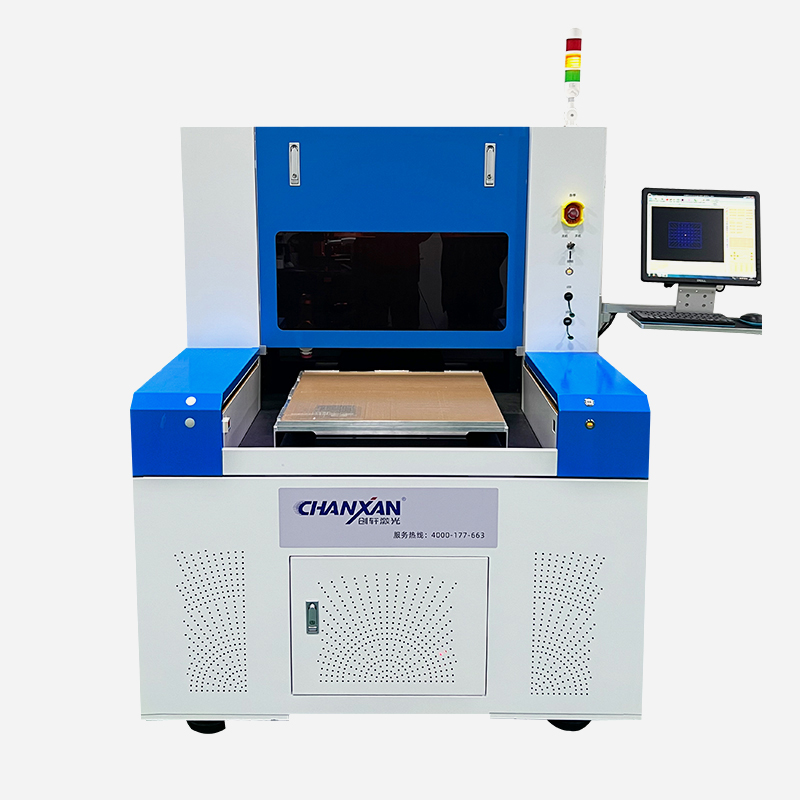
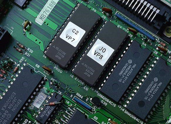
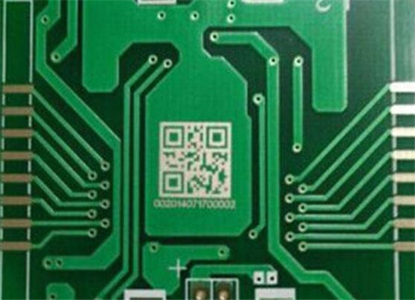
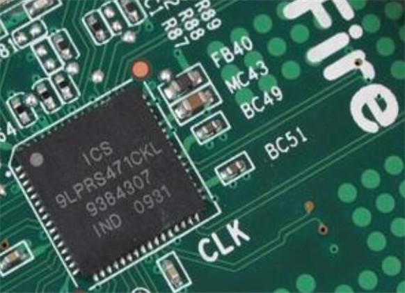
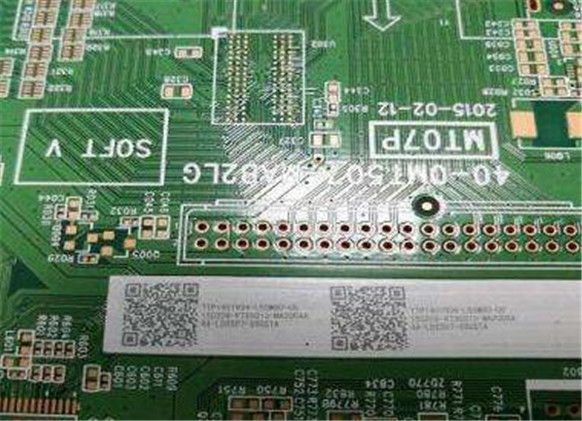
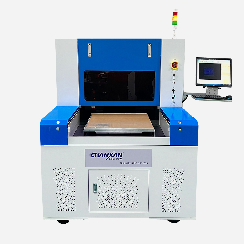
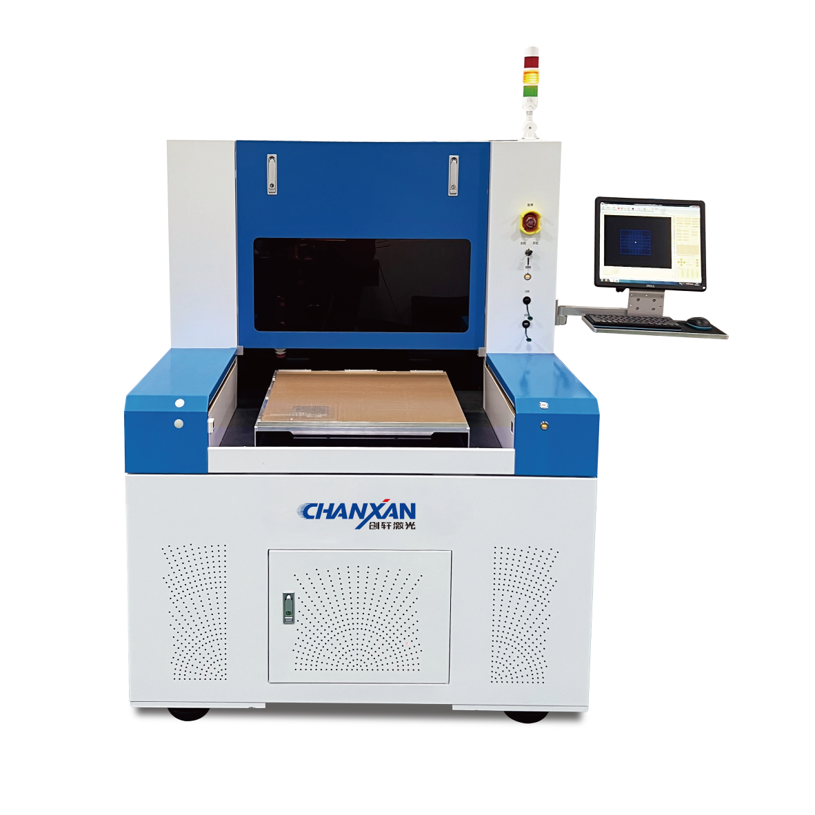
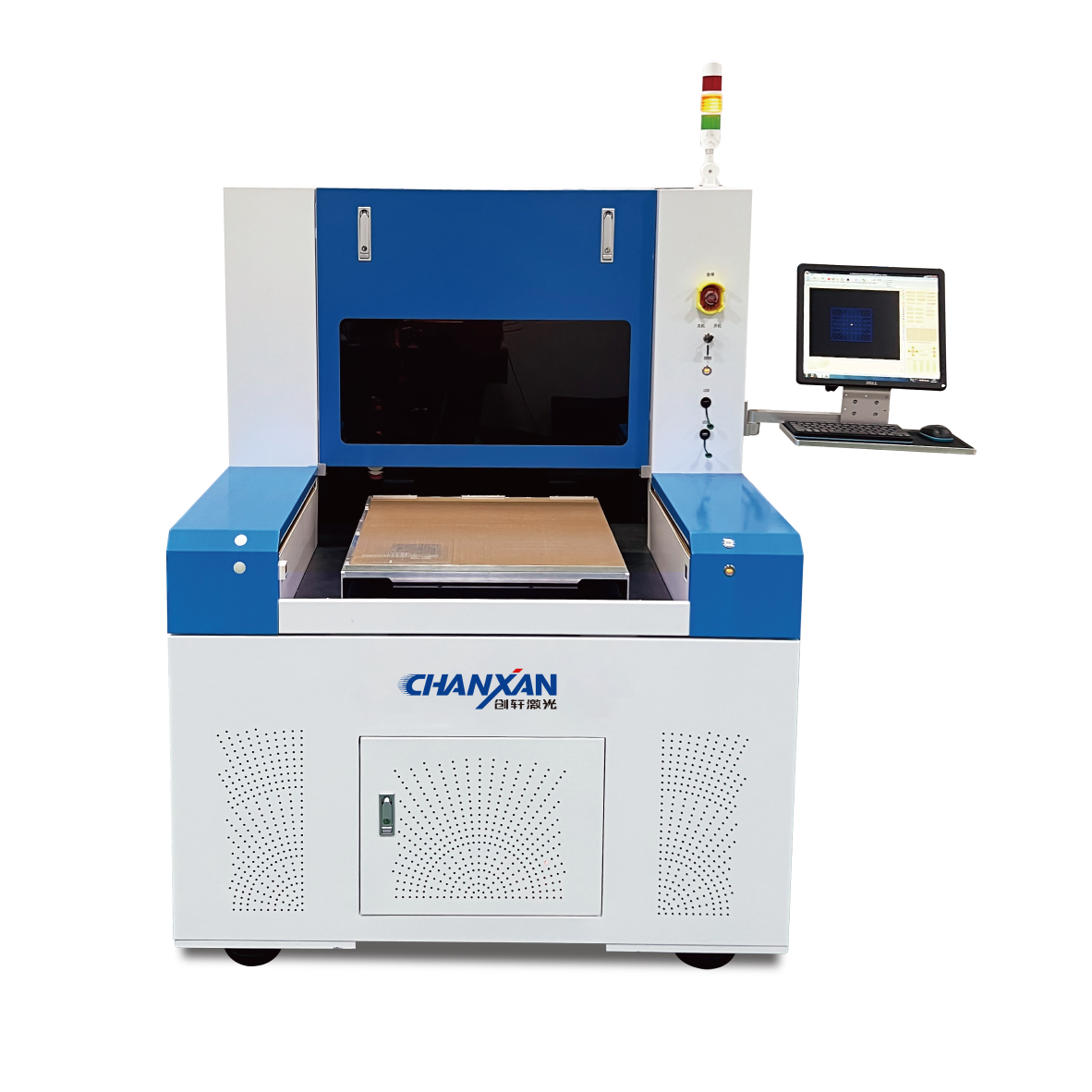
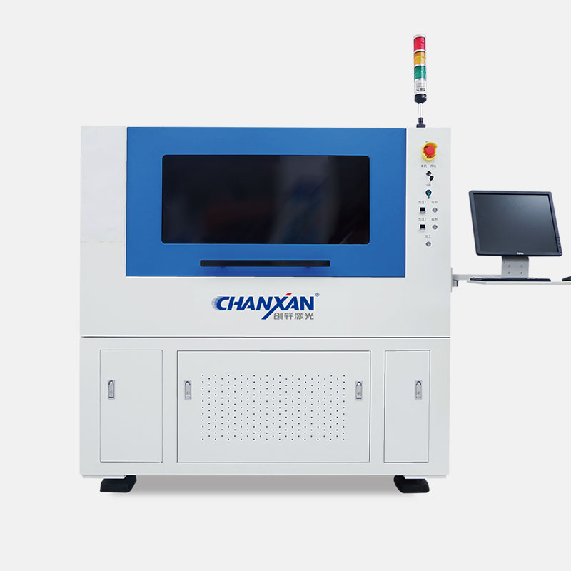
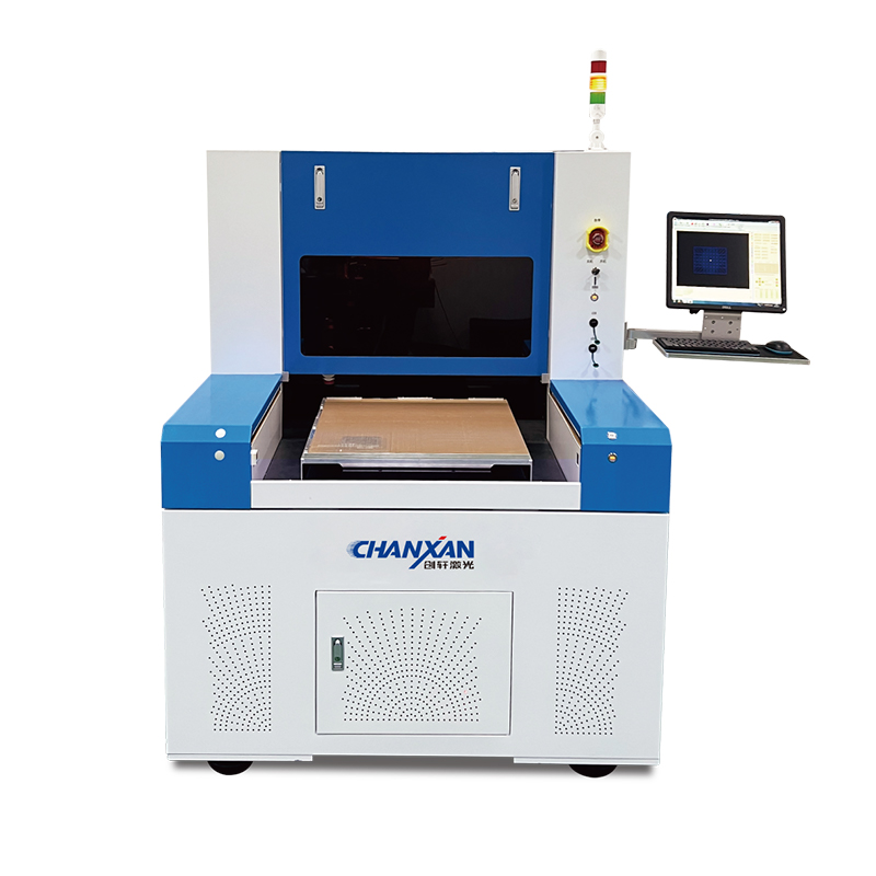
HDI PCB solder mask removal, FPC laser window opening, PCB copper pad exposure, flexible PCB laser cutting, PCB coating removal laser machine
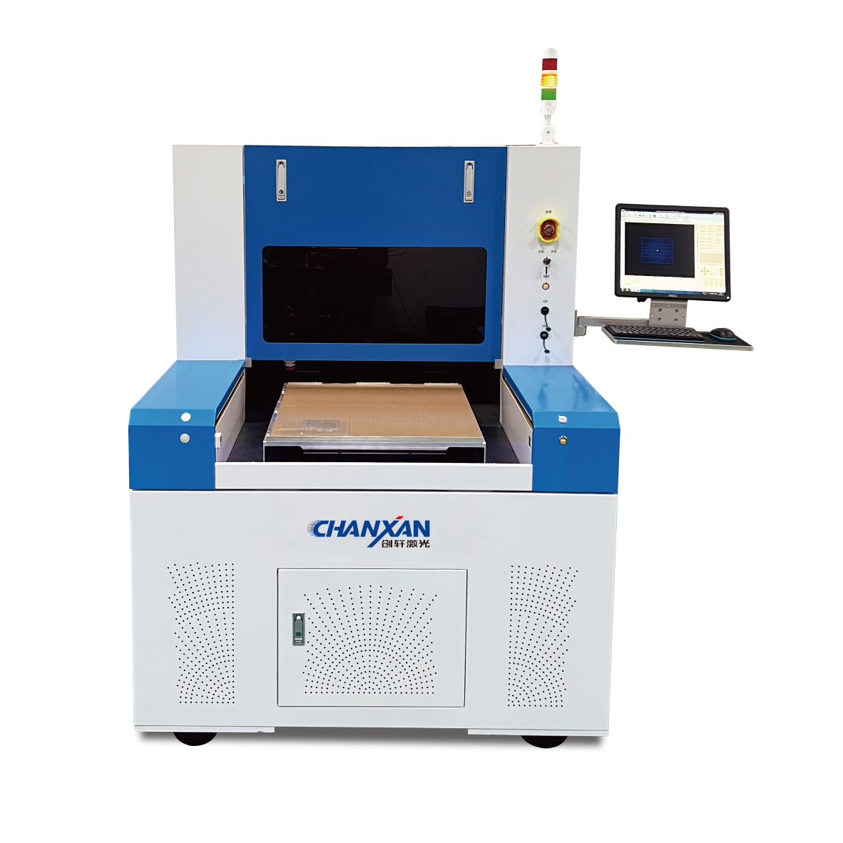
Utilizing ultrashort picosecond pulse technology, it achieves non-thermal ablation with an ultra-low heat-affected zone, ensuring perfect copper protection and clean edge quality. Built for high-end electronics manufacturing, the laser ablation system delivers micron-level accuracy, stable mass production performance, and superior process consistency for HDI, flexible circuits, and semiconductor-grade applications.
In PCB manufacturing, coating removal is used to selectively eliminate solder mask layers and other surface coatings to expose underlying copper pads, enable electrical connections, or prepare bonding areas. Traditional mechanical or chemical methods often introduce contamination, dimensional instability, or substrate damage. The Chanxan Picosecond Laser System is engineered for precise PCB solder mask removal, FPC fine window opening, and high-end selective coating ablation applications. Built on ultrafast picosecond laser technology, the system delivers true "cold processing", enabling non-thermal material removal with virtually no damage to underlying copper traces or dielectric layers. It is designed for advanced electronics manufacturing where zero thermal impact, ultra-clean edges, and micron-level accuracy are required.
Heat-affected zone (HAZ) causing thermal damage
Risk of copper oxidation and substrate delamination
Lower edge quality with potential burrs and debris
Thermal stress accumulation in fine-pitch structures
Limited suitability for advanced HDI and ultra-fine pitch applications
Near-zero heat-affected zone (HAZ) with superior copper protection
Non-thermal ablation eliminates thermal stress and delamination risk
Higher edge quality for micro-scale features with clean, burr-free openings
Ultrashort pulse duration significantly reduces heat diffusion
Ultimate solution for high-end PCB manufacturing where quality outweighs cost
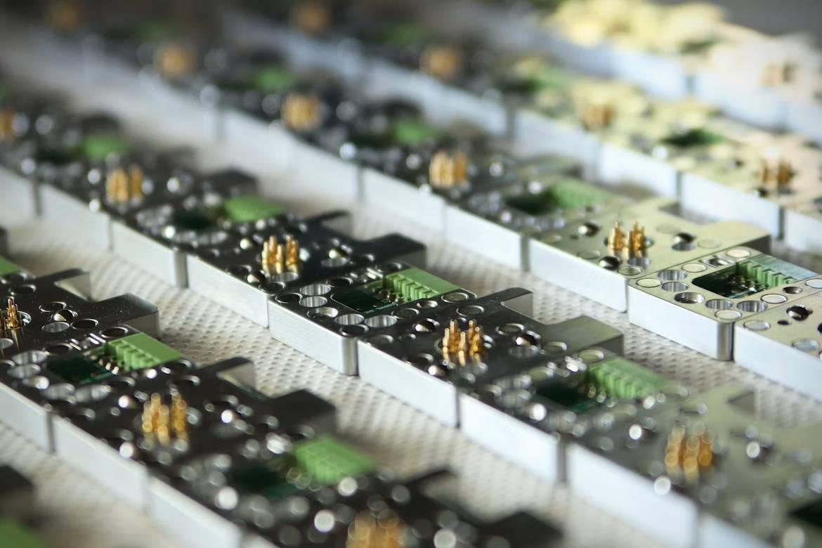
HDI and ultra-fine pitch PCB solder mask opening
High-density copper pad exposure
Advanced multilayer circuit processing
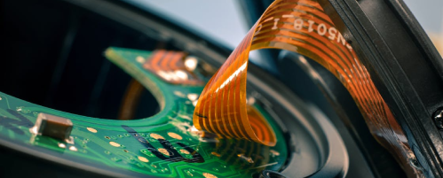
PI film window opening
Flexible circuit patterning
Cover film selective removal
Ceramic substrate structuring
Thin film micro-patterning
Wafer-level processing support
RF module manufacturing
5G communication devices
High-reliability automotive electronics
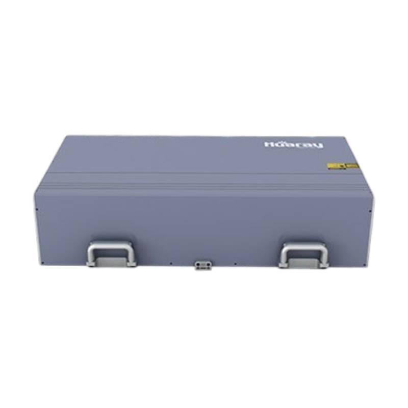
Ultrashort pulse laser output ensures high peak power with minimal thermal diffusion, enabling precise removal of solder mask without substrate damage.
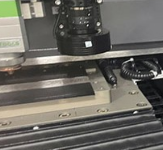
High-speed linear motors combined with marble base structure ensure vibration-free, micron-level stable processing.
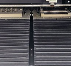
Real-time optical positioning ensures accurate registration of PCB patterns and automatic alignment for complex geometries.
Picosecond pulse duration significantly reduces heat diffusion, enabling clean ablation of solder mask materials without affecting underlying copper or dielectric layers.
The system produces smooth, burr-free opening edges, eliminating the need for secondary cleaning or post-processing.
With ±1μm positioning accuracy and CCD vision alignment, the system supports ultra-fine pad opening and micro-scale patterning on HDI and advanced PCB boards.
Designed for industrial-scale manufacturing, ensuring consistent quality across long production cycles with minimal process variation.
| Item | Specification |
|---|---|
| Model | CW-6050PZ |
| Laser Type | Picosecond UV / IR / Green |
| Laser Power | 30W |
| Working Area | 500 × 500 mm / 600 × 900 mm |
| Adsorption Platform | 1200 × 700 mm (customizable) |
| Positioning Accuracy | ±1 μm |
| Repeatability | ±1 μm |
| Machining Accuracy | ≤30 μm |
| Max Processing Speed | ≤3000 mm/s |
| Machining Thickness | ≤3 mm |
| Motion System | X/Y/Z Three-Axis Linear Motor System |
| Vision System | High-Resolution CCD Alignment |
| Control Software | Chanxan Self-Developed System |
| Supported Formats | PLT, BMP, DXF, DWG, AI, LAS |
| Power Supply | 380V ±10%, 50Hz |
Empowering global manufacturing with 14+ years of expertise, dual CE & ISO certified quality, over 100 national patents, and a comprehensive Technical Training Service designed for your operational success.
Systematic Training: Comprehensive full-process skill coverage.
Expert Support: Continuous project follow-up by senior engineers.
Multiple Formats: Flexible learning modes to maximize operational efficiency.
Outcome Driven: Empowering clients from "knowing" to "mastering" technology.
24H Fast Response: Technical diagnosis and solutions within 24 hours.
Warranty Policy: 1-year machine warranty with lifetime technical support.
Global Parts Supply: Rapid delivery of original parts via global network.
Lifecycle Care: From installation to long-term maintenance and software upgrades.
In-depth analysis of your specific material and performance requirements.
Precision laser sampling to verify the feasibility of the technical solution.
Bespoke manufacturing under ISO9001 quality management systems.
Final testing, professional wooden packing, and secure global shipment.
We are seeking professional partners to expand our presence in the global industrial laser market. Scale your business with Chanxan's high-end technology and manufacturing strength.
Become an AgentApplications
Subscriber:Picosecond PCB Solder Mask Removal Laser Machine