Key Words: Silicon Wafer Dicing PCB Depaneling Glass Cutting
Home > Products > Laser Micromachining Systems
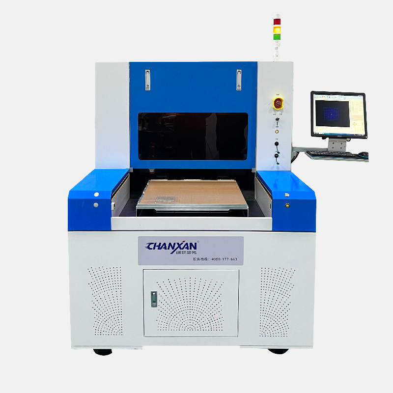


Cold laser cutting for thin metal foil & semiconductor packaging
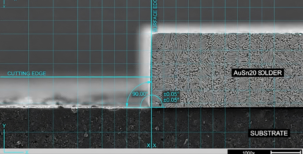
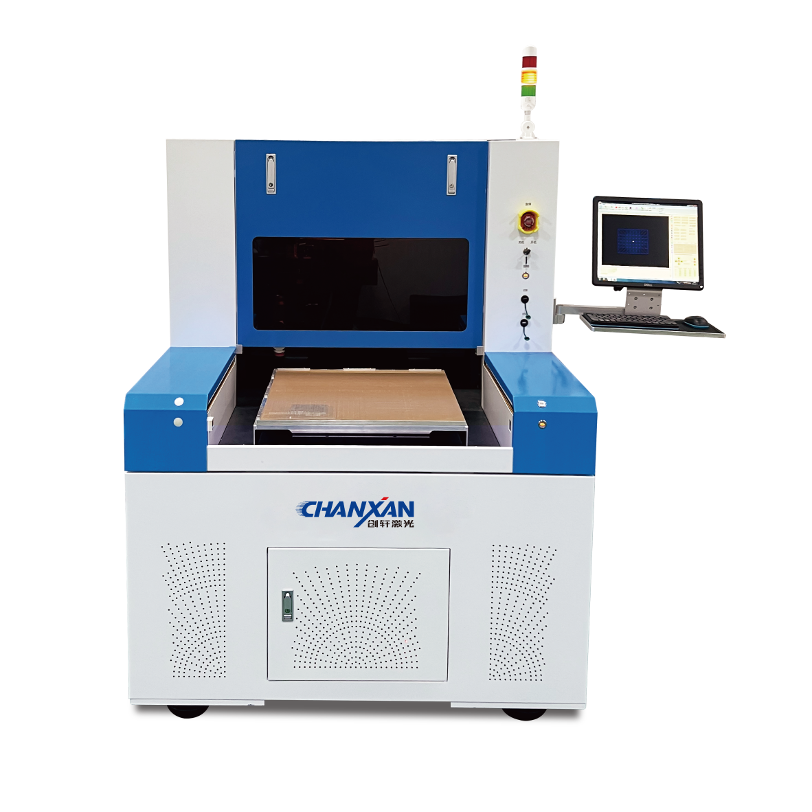
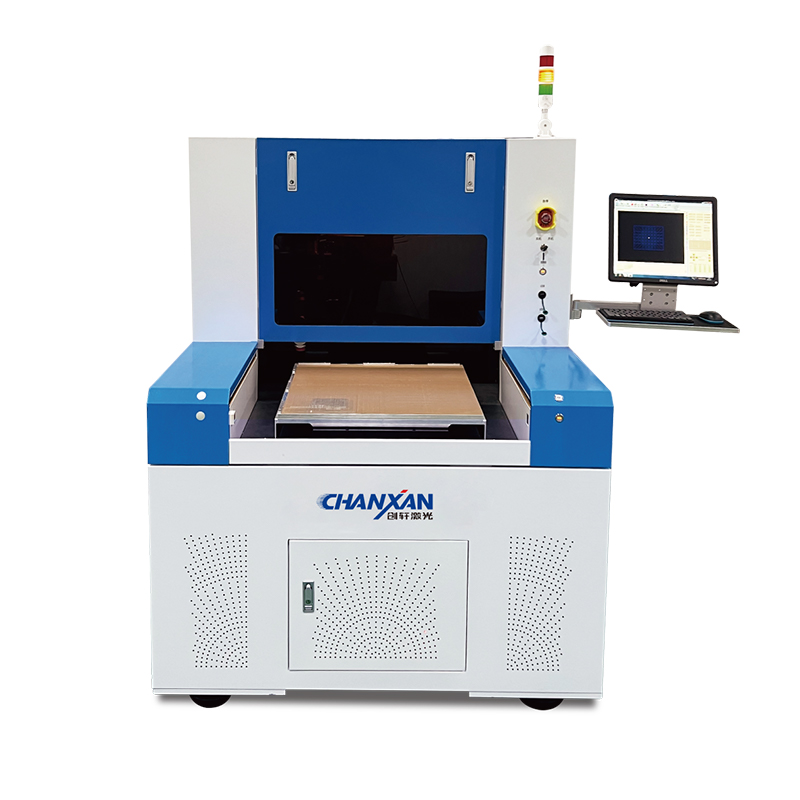
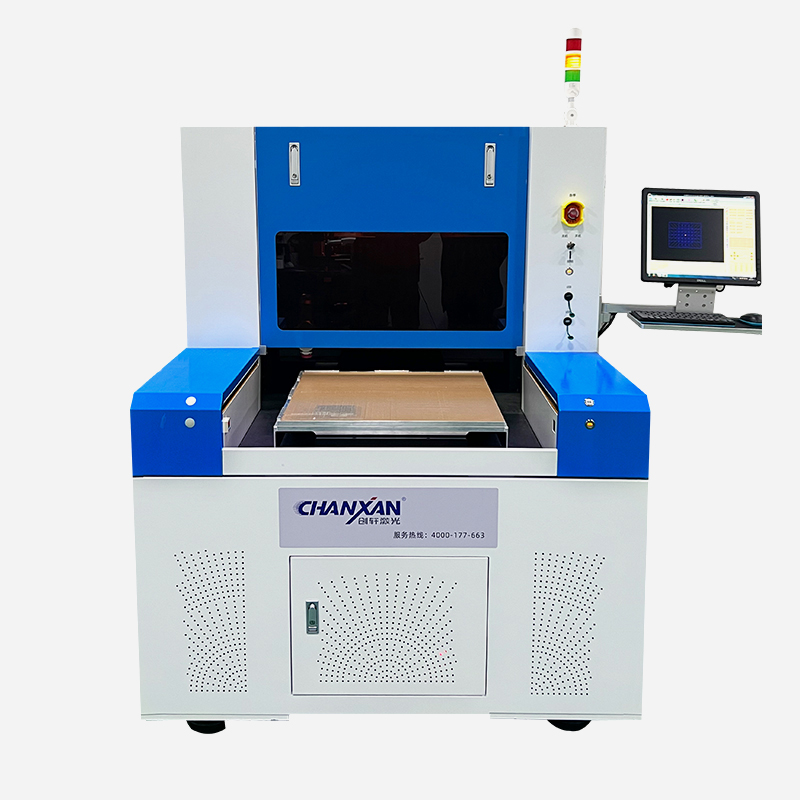
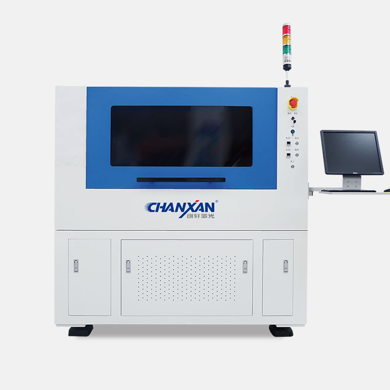
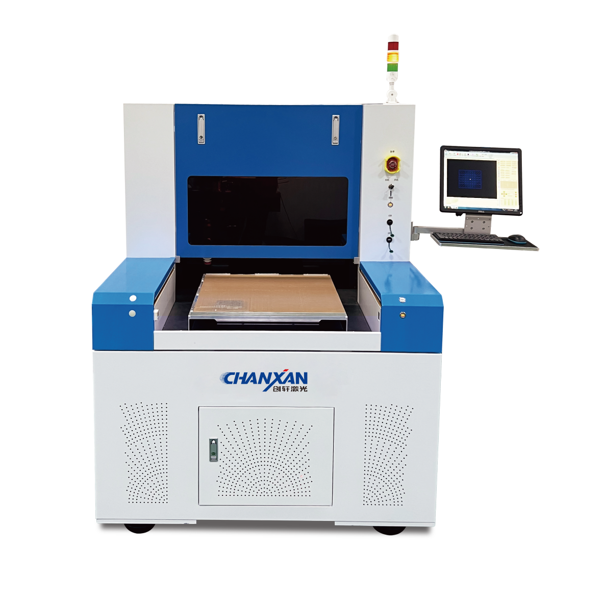
Our picosecond laser cutting machine delivers cold ablation with minimal heat-affected zone, avoiding thermal deformation and edge burns on delicate materials. It achieves burr-free precision cutting for semiconductor solder preforms and thin metal foils, equipped with CCD vision positioning for high repeat accuracy. Stable performance supports continuous running for mass production, widely used in electronics and semiconductor manufacturing lines.
Clean Edge • Minimal HAZ • Stable Production
< 2 μm HAZ Verified
Ra < 0.1 μm Edge
99.8% Packaging Yield
Instant proof of cold athermal ablation across 4 core packaging substrates.
Sub‑micron hardware engineered for 24/7 fab packaging lines.
< 10 ps pulse eliminates all thermal heat-affected zone.
Thermal Disruption < 2 µmCoaxial telecentric vision with ±1.0 µm fiducial lock.
Fiducial Accuracy ±1 µmClass 00 natural granite isolates cleanroom vibration.
Cleanroom Vibration IsolationIronless direct-drive delivering up to 3000 mm/s speed.
Max Speed 3000 mm/sSide‑by‑side microscopic comparison proving dramatic yield improvements.
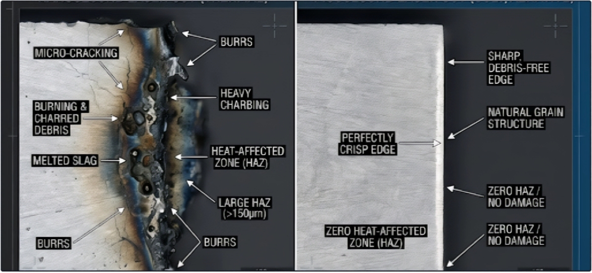
Heavy Slag & Burrs
HAZ > 80 μm Micro‑Cracks
High Post‑Process Cost
Clean Edge (Ra < 0.1 μm)
Minimal HAZ (< 2 μm)
Zero Post‑Deburring
Proven in high-reliability semiconductor packaging and SMT cleanrooms.
Wafer-level die attach solder preform singulation.
High-speed SMT micro-circuit substrate fabrication.
Ultra-thin precision alloy foil stamping replacement.
Essential parameters for cleanroom equipment procurement.
| Item | Specification |
|---|---|
| Laser Type | Picosecond |
| Working Area | 500 × 610 mm |
| Positioning Accuracy | ±1 μm |
| Processing Speed | Max 3,000 mm/s |
| Focus Spot | ≤ 20 μm |
| Warranty | 12 Months |
Get free sample‑cut evaluation, quotation and technical support for our picosecond laser cutting system.
Go To Contact Us Page →Submit your material requirements & CAD drawings on contact page
Applications
Subscriber:Precision Picosecond Laser Cutting Machine for Semiconductor Solder Preform