Key Words: Silicon Wafer Dicing PCB Depaneling Glass Cutting
Home > News > Industry News
【Description】:
Discover how UV picosecond laser systems achieve damage-free PCB coating & solder mask removal with micron-level precision and self-limiting depth control.
Removing solder mask, conformal coating, or coverlay material from a printed circuit board sounds simple on paper — until the goal is to expose a copper pad or trace underneath without touching the copper itself. Whether it's rework and repair, selective solder mask opening for fine-pitch components, or conformal coating removal for testing and rework, the margin for error is often measured in microns. Scratch or thin the copper, and the board is either scrapped or its long-term reliability is compromised.
Among the available techniques — mechanical scraping, chemical solvents, thermal stripping, plasma etching, and laser ablation — pulsed UV laser ablation, and increasingly picosecond laser ablation, has emerged as the most precise method for selectively removing PCB coatings while leaving the underlying copper intact.
PCB coatings exist specifically to protect copper traces and components from moisture, dust, chemical exposure, and mechanical damage. Common coating types include:
Solder mask — the permanent protective layer covering most of the board
Conformal coatings — acrylic, silicone, urethane, and epoxy coatings applied over populated boards for environmental protection
Parylene — a vapor-deposited conformal coating valued for chemical resistance and biocompatibility, common in medical and aerospace electronics
Coverlay — the flexible circuit equivalent of solder mask, used on polyimide-based flex and rigid-flex PCBs
Whenever a component needs to be reworked, tested, or replaced, or when a fine-pitch pad needs to be selectively exposed, some or all of that coating has to come off — precisely, and only in the targeted area. Damage the copper underneath, and you risk lifted pads, reduced trace cross-section, weakened solder joints, or an outright short.
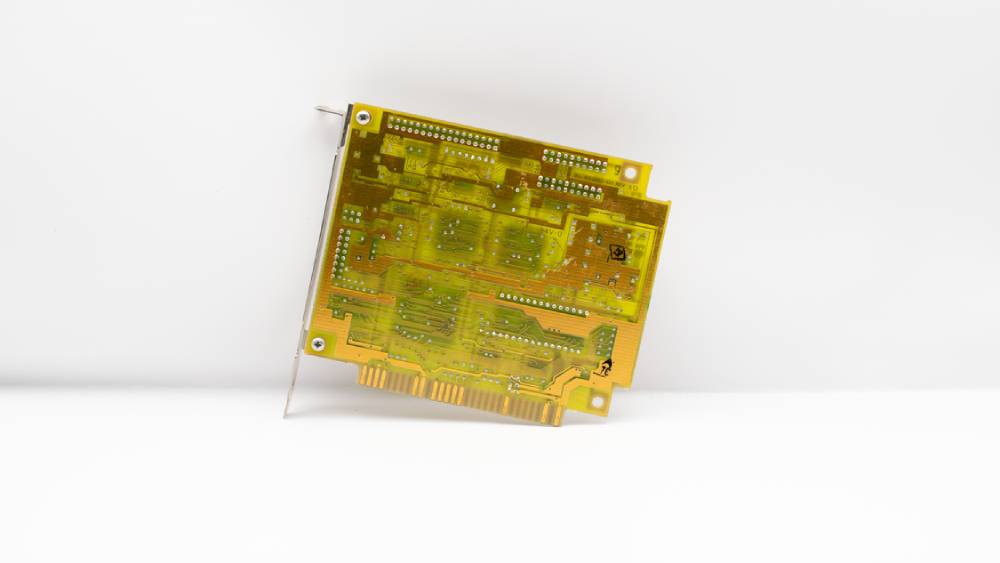
Mechanical removal (scraping, sanding, or abrasive blasting) physically contacts the board surface, which risks scratching or thinning copper traces, especially on fine-pitch or flex circuits. Automotive-grade rework standards typically cap sandblasting pressure well below levels that would risk trace fracture, which itself signals how easily this method can cross the line into copper damage.
Chemical solvent stripping works well for bulk removal of acrylic, silicone, or urethane coatings but is inherently imprecise for localized, small-area rework — solvents spread beyond the intended area, and chemically inert coatings like Parylene resist solvents almost entirely.
Thermal stripping (hot air guns, heated scrapers) can soften coatings for removal, but the heat input is difficult to confine to a small spot, creating risk of thermal stress to nearby components and, on thin flex substrates, to the copper itself.
Plasma etching is effective for full-board Parylene removal but is a whole-part, batch-style process — it's not a selective, spot-rework tool.
This leaves laser ablation as the only method that combines high spatial precision (down to single-micron control) with selective, programmable targeting of just the coated area that needs to be removed.
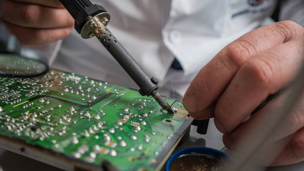
The precision of laser coating removal comes down to a physical principle: different materials have different ablation thresholds — the minimum energy density (fluence) needed to vaporize or break down that material. Organic coatings like solder mask, acrylic, silicone, urethane, and Parylene have a much lower ablation threshold than metallic copper. By tuning the laser's wavelength, pulse duration, and fluence to sit just above the coating's ablation threshold but well below copper's, the laser removes the coating and then — critically — stops.
UV wavelengths (commonly 355 nm) are strongly absorbed by the organic bonds in most conformal coatings and solder masks, while being far less efficiently absorbed by copper. This wavelength-dependent absorption difference is a major reason UV lasers are the default choice for coating removal work: the coating absorbs and ablates efficiently, while copper reflects a much larger share of the same wavelength.
Pulsed UV lasers with nanosecond-scale, and increasingly picosecond and even sub-nanosecond pulse durations, deposit energy faster than heat can diffuse into the underlying copper. This keeps the interaction confined to the coating layer itself, rather than allowing thermal effects to spread downward and damage the metal beneath. Research on short-pulse UV laser removal of Parylene coatings has shown that below roughly 1 nanosecond pulse duration, laser fluence can be tuned so precisely that removal mechanisms shift from thermal ablation to more controlled, low-damage material removal — giving process engineers finer control over exactly how much material is removed and where the process stops.
Because the coating's ablation threshold sits well below copper's, a properly tuned laser process becomes effectively self-limiting: once the coating is removed and the beam reaches the copper surface, the fluence delivered is no longer sufficient to ablate the metal. This same threshold-difference principle has been demonstrated even in ultra-precision applications like nanoscale copper oxide removal in integrated circuits, where femtosecond lasers tuned below copper's ablation threshold were used to strip a surface oxide layer while leaving the underlying bulk copper untouched — the same fundamental physics that makes laser coating removal on PCBs so precise, just at an even finer scale.
Unlike solvents or plasma etching, laser ablation is fully programmable — the beam only touches the exact area defined by the CAD pattern or rework outline, whether that's a single pad, a small cluster of components, or a defined cavity for a cutout. This is the basis of what the industry calls laser skiving: selectively removing a defined layer — solder mask, coverlay, or dry film — down to a target depth, including exposing copper pads on flex circuits too small or too tightly spaced for mechanical drilling.
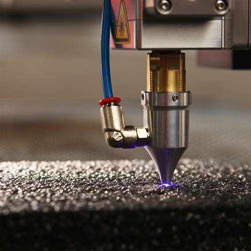
Published process work on UV laser coating removal gives a useful sense of the operating window:
Fluence range: roughly 0.4–0.7 J/cm² is typical for efficient Parylene removal without impacting the underlying substrate, though the exact number depends on coating thickness and material
Coating thickness handled: Parylene coatings in the 3–30 micron range are commonly processed with pulsed UV lasers at micron-level removal precision
Multi-pass strategy: for thicker coatings or where charring must be minimized, multiple lower-fluence passes — rather than a single high-fluence pass — combined with assist gas and controlled scan intervals reduce heat accumulation and improve edge quality
PCB rework and repair — selectively exposing a solder pad or trace for component replacement without disturbing surrounding coating or copper
Solder mask opening for fine-pitch components — precision exposure of pads too small or tightly spaced for traditional masking and etching
Medical and aerospace electronics — Parylene removal on high-reliability boards where substrate integrity cannot be compromised
Flex and rigid-flex circuits — coverlay removal and copper pad exposure via laser skiving, particularly where pad spacing is too fine for mechanical drilling
Cavity formation — controlled, depth-limited material removal down to a defined layer, without fully cutting through the board
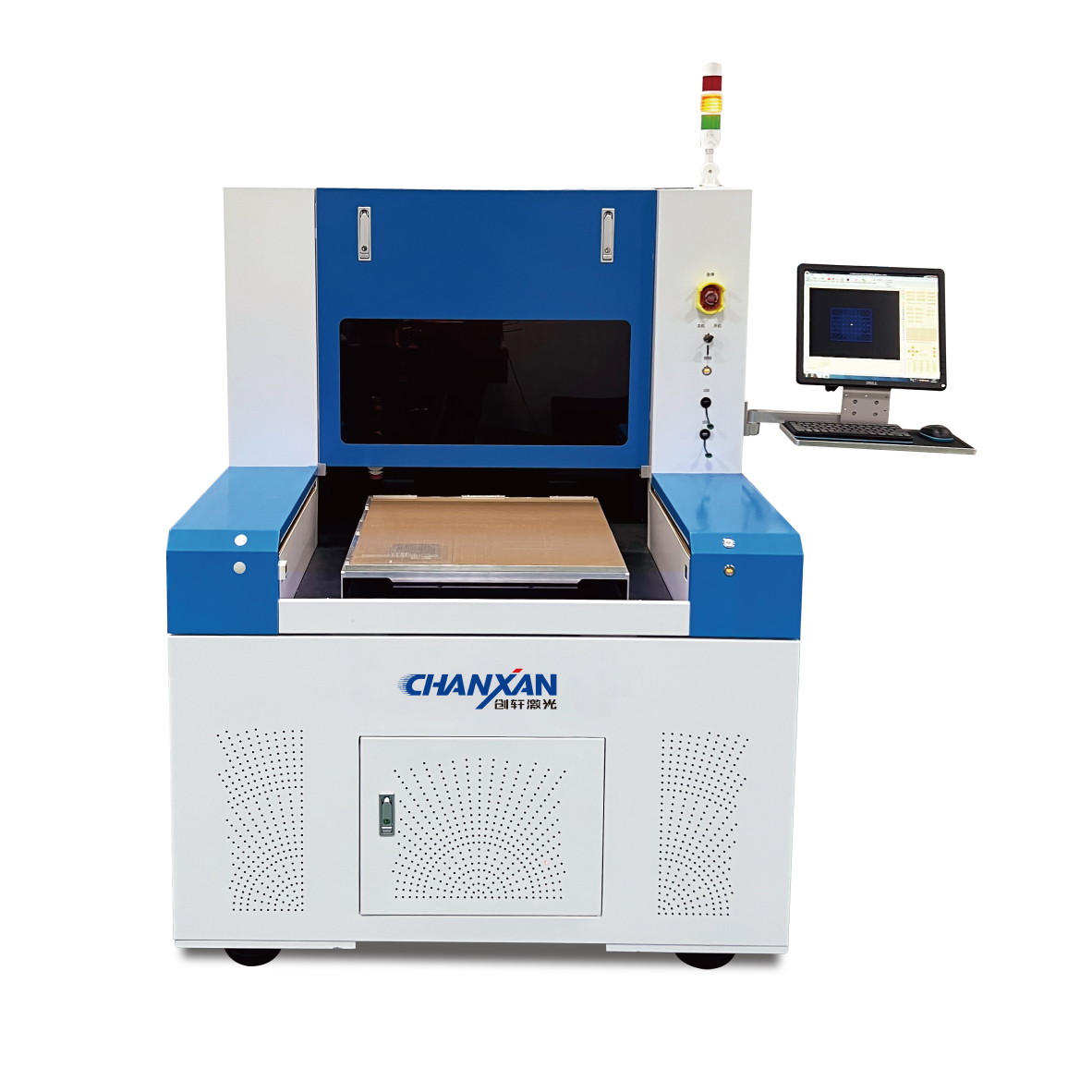
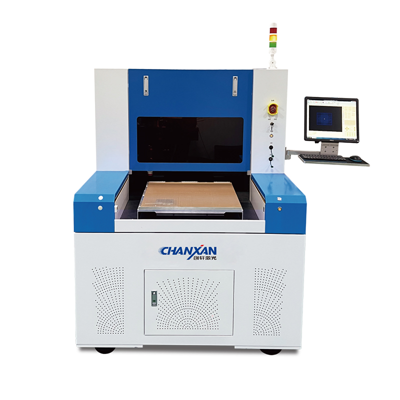
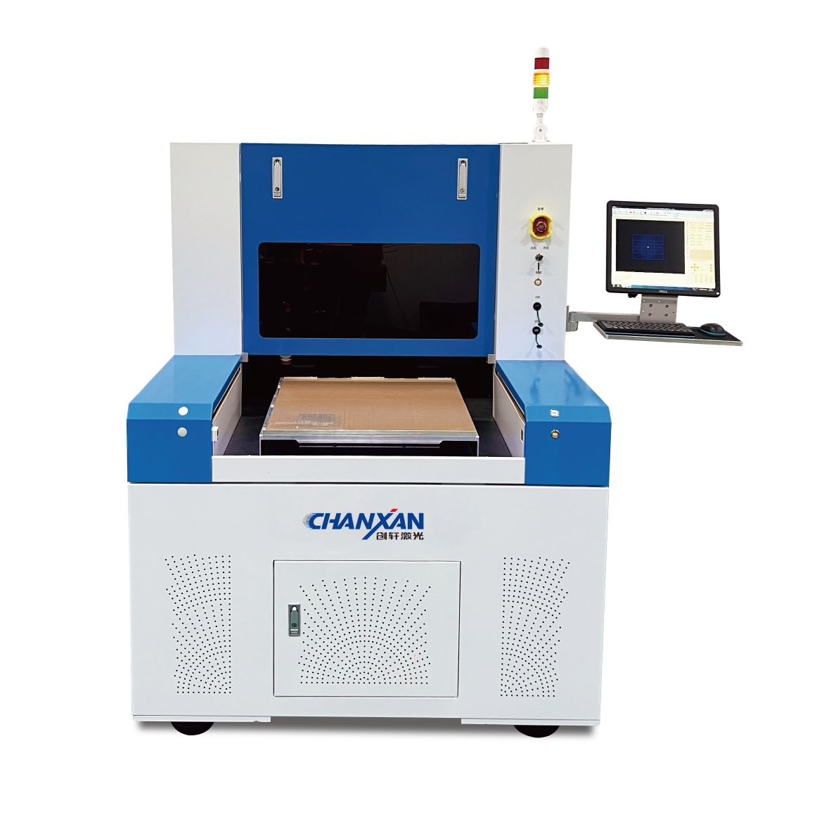
For PCB manufacturers and rework facilities looking to move coating removal away from solvents, thermal stripping, or mechanical abrasion, Chanxan's UV and picosecond laser platforms are built around exactly this kind of selective, damage-free material removal.
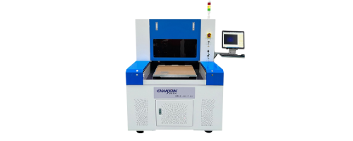
Key capabilities relevant to coating removal applications include:
355 nm UV laser sources tuned for efficient absorption in solder mask, conformal coatings, and Parylene, with minimal copper interaction
Picosecond pulse options for applications demanding the tightest possible control over heat-affected zone and removal depth, particularly on thin coatings near sensitive copper pads
Programmable fluence and multi-pass scan control, allowing engineers to dial in a process window that reliably clears the coating layer while staying below copper's ablation threshold
Vision-guided alignment for pinpoint targeting on rework jobs, fine-pitch pad exposure, and small-batch repair work
Depth-controlled skiving profiles for cavity formation and layer-selective removal on both rigid and flex PCB constructions
Whether the application is high-volume solder mask opening on a production line or delicate Parylene removal on a single high-value aerospace board, a Chanxan laser system gives process engineers the fluence precision and beam control needed to remove exactly what needs to come off — and nothing more.
When the requirement is to remove PCB coating without so much as scratching the copper underneath, mechanical, chemical, and thermal methods all struggle to combine precision with selectivity. Laser ablation — particularly UV and picosecond laser systems tuned to exploit the ablation threshold gap between organic coatings and copper — remains the most precise method available, capable of confining material removal to single-micron accuracy while leaving the underlying metal untouched. As PCB designs continue toward finer pitches and higher reliability requirements, laser-based coating removal platforms like Chanxan's are positioned to be the standard tool for this kind of precision rework and production work.
Evaluating a laser-based coating removal process for your PCB rework or production line?
Contact Chanxan Expert Team| Free solution
Previous: Precision Technical Glass Laser Processing Solution
Next: Picosecond Laser Direct Writing of Laser-Induced Graphene Electrodes on Polyimide Films