Key Words: Silicon Wafer Dicing PCB Depaneling Glass Cutting
Home > News > Industry News
【Description】:
Precision Laser Cutting & Micromachining for Flexible Films
High-precision laser cutting, drilling, coating removal, and patterning solutions for polyimide, polyester, polypropylene, Mylar, LCP, flexible PCB, and advanced thin-film materials.
Conventional methods like mechanical die punching, rotary cutting, and blade slitting inflict severe physical stress on delicate films, leading to costly manufacturing bottlenecks:
Burr formation and frayed edge fibers
Material deformation and non-linear stretching
Trace delamination in multi-layer composites
Dust contamination impacting cleanroom limits
Limited geometry flexibility for complex designs
High tool wear and continuous replacement costs
Migrating to non-contact ultrafast and UV laser processing resolves mechanical shear issues, offering a fully digital, stress-free manufacturing workflow:
Non-contact processing eliminates physical stress
Minimal Heat-Affected Zone (HAZ) prevents melting
Pristine, burr-free cutting on ultra-thin films
Zero tooling cost and instant CAD profile switching
Micro-scale precision (10-20 um tolerances)
Complex contour capability for advanced nesting
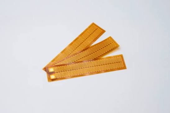
Polyimide films are fundamental to modern electronics, frequently utilized as insulation films, thermal management layers, and electronic shielding materials. When executing polyimide laser cutting, our systems utilize ultrafast cold ablation to deliver pristine edges without carbonization. This technique allows for complex laser cut kapton contours and flawless laser cut kapton tape profiles crucial for flexible circuits. Beyond standard pi cutting, our equipment integrates advanced laser drilling capabilities, generating micro holes and micro vias with sub-micron accuracy, ensuring reliable high-density interconnects without thermal deformation.
Explore Polyimide Solutions →
Widely deployed across flexible displays, protective films, and electronic insulation layers, polyester requires strict thermal management to prevent edge melting. Our advanced optics optimize laser cut polyester processes, ensuring clean edges and absolutely no fraying. Whether you require high-speed pet film laser cutting for packaging or intricate laser cutting mylar workflows for precision Mylar stencils, the non-contact beam eliminates tearing. By integrating sophisticated precision laser cutting and selective laser marking and micro engraving techniques, we maintain optical clarity and structural integrity even on the thinnest transparent substrates.
View PET Processing →
Polypropylene is heavily favored in packaging films, battery separators, and industrial thin sheets due to its chemical resistance. Executing a clean laser cut polypropylene profile demands a perfectly tuned wavelength to prevent material localized burning. Our digital routing allows for rapid laser cut polypropylene sheet processing, effortlessly handling complex contour shapes that would snap mechanical blades. Through refined precision laser cutting and rapid laser drilling, we achieve exact precision openings and edge trimming, preserving the critical microscopic porosity required for advanced EV battery applications.
Discover PP Cutting Capabilities →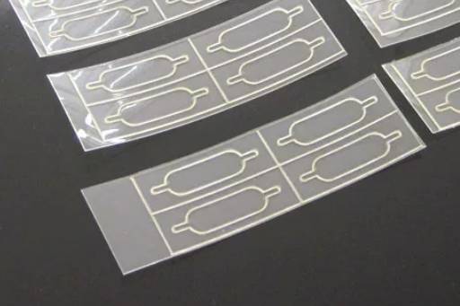
Liquid Crystal Polymer (LCP) is the backbone of high-frequency electronics, RF components, and next-generation semiconductor packaging. The extreme densification of 5G antennas necessitates an immaculate lcp laser cut. Because LCP is sensitive to micro-cracking under physical pressure, our lcp laser cut processing utilizes ultra-short pulse (USP) technology to bypass mechanical impact entirely. We deploy high-end laser micromachining and laser drilling to execute flawless micro vias and dense signal routing channels, safeguarding the material's low dielectric constant.
Read LCP Processing Studies →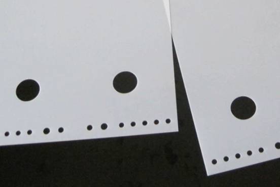
PTFE films are widely used in semiconductor insulation, medical devices, aerospace components, and chemical sealing applications. Traditional die cutting often causes burrs, deformation, and inconsistent edge quality on thin PTFE materials. Our laser systems enable precision PTFE laser cutting with virtually no mechanical stress, producing clean edges and intricate geometries without material distortion. By combining advanced laser micromachining and laser drilling technologies, we create micro holes, slots, and complex profiles while maintaining tight tolerances and excellent surface quality.
Explore PTFE Processing Solutions →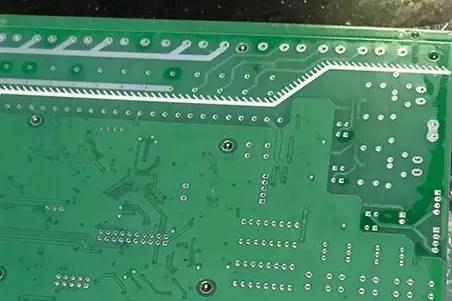
During electronics manufacturing, PCB repair, and rework processes, engineers must often expose localized copper testing pads hidden beneath thick protective barriers. Precision pcb coating removal replaces toxic chemical solvents and abrasive mechanical scraping. By utilizing controlled laser ablation and coating removal techniques, our systems strip conformal coatings and tough insulation resins layer-by-layer. This selective ablation process cleans specific geometries perfectly, preparing the flex PCB for re-soldering or diagnostic probing without inducing any thermal damage to the fragile active components below.
Learn About Selective Laser Ablation →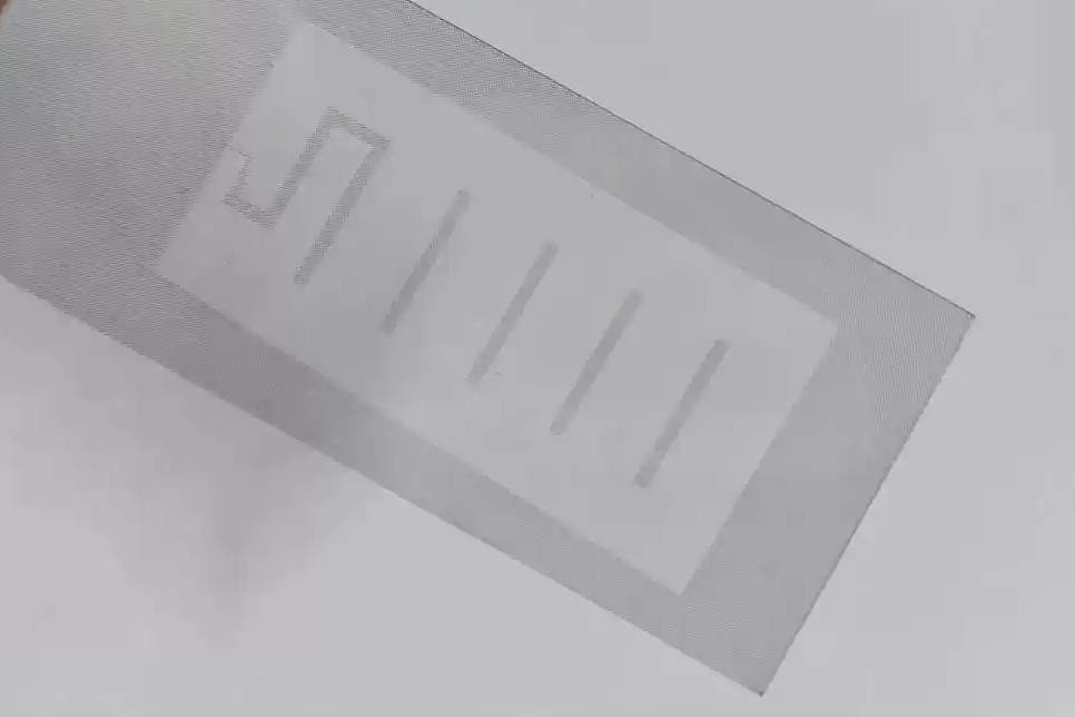
Indium Tin Oxide (ITO) coated films are essential for touch panels, flexible displays, and transparent conductive electronics. Successful ito laser patterning requires selectively stripping the conductive microscopic layer without damaging the underlying PET or glass substrate. Our specialized optical systems execute precision laser patterning and laser ablation, selectively evaporating the ITO layer to isolate circuits with single-digit micron isolation gaps. This ensures perfect electrical functionality and maintains high visual transparency without leaving conductive dross behind.
Explore ITO Patterning Details →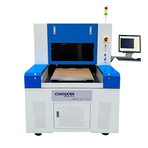
The ultimate micro-machining system, featuring configurable UV, Green, and IR laser sources with femtosecond, picosecond, or nanosecond pulse options tailored to precision needs. Designed for true non-thermal cold ablation of ultra-thin films and advanced polymers, with optional roll-to-sheet production capability.
Rapid flex pcb laser cutting throughput
Automated compensation for substrate shrinkage
Vibration-damped granite structural core
Ideal for PET, Mylar, and rigid-flex separation
A high-performance, cost-effective manufacturing platform equipped with an advanced RF CO₂ laser engine. Designed for high-volume production, it delivers rapid processing speeds and smooth edge profiles for insulating layers, polymers, and protective films. The system supports complex kiss-cutting and full-cutting tasks with micro-level accuracy.
Non-contact, burr-free processing for delicate films
Advanced CCD vision alignment for repeatable geometry
High-speed servo motor system for efficient batch manufacturing
Stable RF CO2 source ensures consistent thermal output and minimal HAZ
| Material | Optimal Process | Typical Industrial Use |
|---|---|---|
| PI Film | Precision Cutting / Drilling | Flexible Circuits, Thermal Management |
| PET Film | High-Speed Cutting | Display Insulation, Protective Covers |
| PTFE | Micro Drilling / Cutting | Medical filtration membranes, Aerospace Electronics |
| Mylar | Stencil Cutting / Edge Trimming | SMT Masking, Insulation Sheets |
| LCP | Laser Micromachining | 5G RF Devices, High-Frequency Antennas |
| ITO Film | Laser Patterning / Ablation | Touch Panels, Transparent Conductors |
Consistently achieving ±10µm to ±20µm tolerances for critical high-density electronic assemblies.
Built on granite bases with industrial-grade chillers for uninterrupted 24/7 commercial production runs.
Vision-guided dynamic coordinate tracking eliminates reject rates caused by material deformation.
Comprehensive in-house lab validation ensures the laser parameters perfectly match your exact polymer mix.
End-to-end industrial production support, from localized installation to lifetime software calibration.
In-depth analysis of your specific material and performance requirements.
Precision laser sampling to verify the feasibility of the technical solution.
Bespoke manufacturing under ISO9001 quality management systems.
Final testing, professional wooden packing, and secure global shipment.
Yes. By utilizing an ultra-short pulse (USP) UV laser, energy is delivered via non-thermal cold ablation. This breaks the molecular bonds instantly, completely preventing heat accumulation, edge burning, or carbonized soot.
A solid-state Ultraviolet (355nm) picosecond or femtosecond laser is the industry standard for polyimide. It provides the necessary photon energy to execute burr-free cuts while ensuring a near-zero heat-affected zone (HAZ).
Absolutely. PET and Mylar films cut exceptionally well with correctly tuned laser frequencies. The process yields perfectly sealed, transparent edges with no fraying, making it ideal for stencils and display films.
It is the preferred method for modern high-density flex PCBs. Lasers replace expensive hard tooling dies, bypass mechanical shear stresses that cause trace delamination, and allow for extreme component nesting density.
Advanced digital galvanometer scanners paired with high-resolution machine vision registration allow industrial laser workstations to maintain positioning and cutting precision within ±10 to ±20 µm consistently.
Our systems process a wide range of flexible substrates including Polyimide (PI), PET, Polypropylene (PP), LCP, Teflon (PTFE), FR4, copper-clad laminates, and advanced transparent conductive films like ITO.
Yes. Laser ablation can be depth-controlled at the micron level to selectively strip conformal insulation layers or coverlays off specific copper pads without inducing thermal damage to the underlying active board.
Industrial laser systems can easily process Mylar films ranging from ultra-thin 10µm foils up to thick 500µm rigid stencil sheets, adjusting pulse overlap and power settings to maintain a pristine edge.
Send your material type, thickness, and CAD drawing files. Our applications engineers will recommend the optimal laser wavelength, process your material in our lab, and provide detailed sample testing reports.
| Free solution
Previous: Polyimide (PI) Laser Cutting for Flexible PCB Manufacturing
Next: Why Is UV Laser Cutting Preferred Over Mechanical Die Punching for Flex PCB Laser Cutting?