Key Words: Silicon Wafer Dicing PCB Depaneling Glass Cutting
Home > News > Industry News
【Description】:
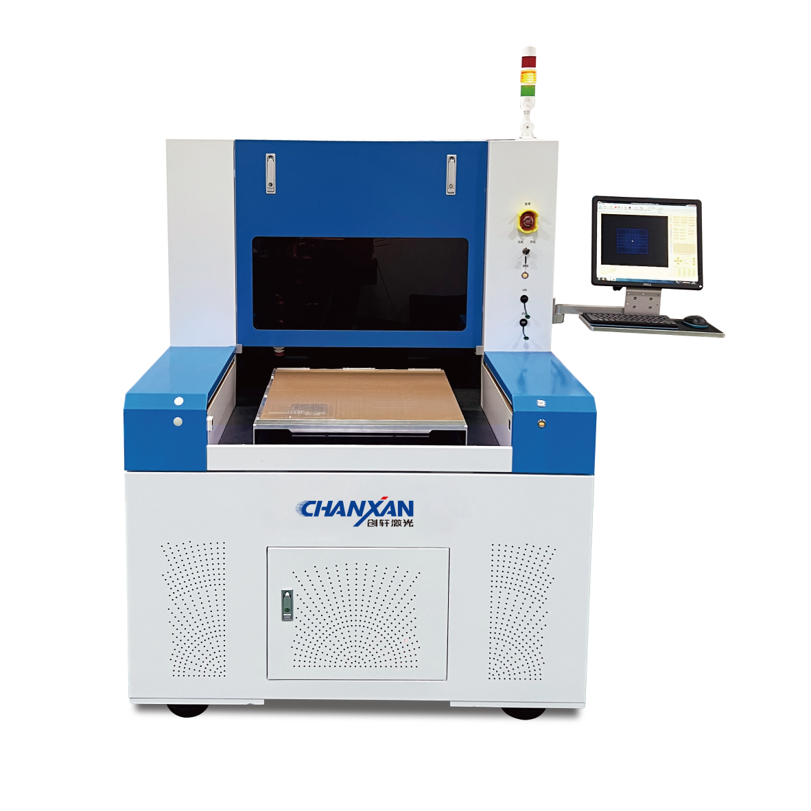
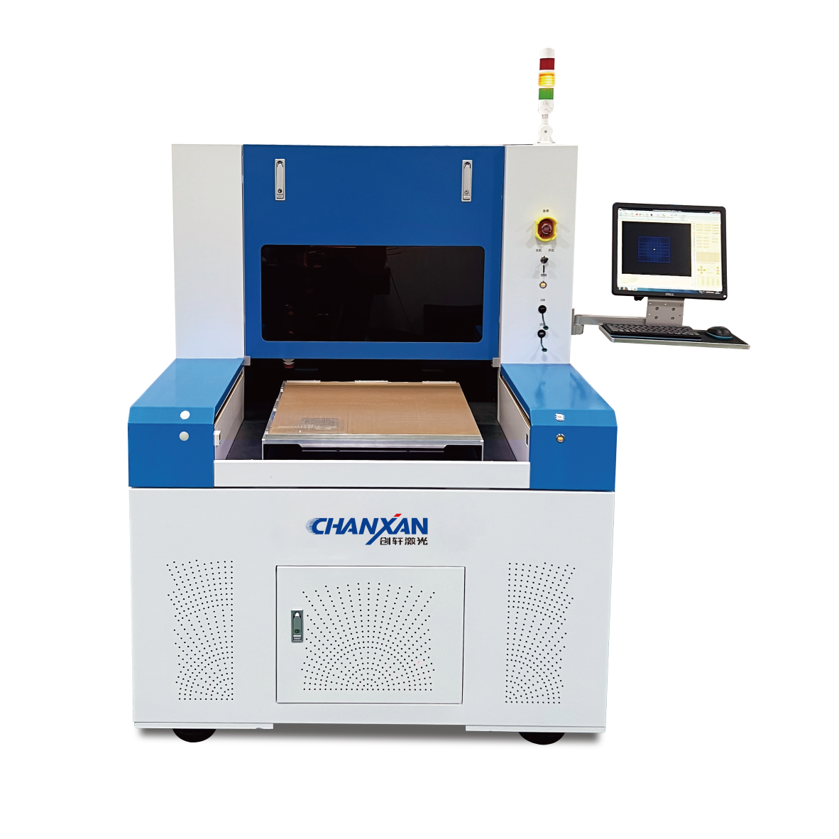
Chanxan picosecond laser wafer dicing machine delivers <200 nm sidewall damage & 5 μm kerf width for GaN-on-Si & GaN-on-Sapphire.
Gallium nitride (GaN) has rapidly transitioned from a research curiosity to a mainstream semiconductor material, powering:
RF power amplifiers for 5G/6G infrastructure
High-electron-mobility transistors (HEMTs) for power conversion
Micro-LED displays and visible light communication
LiDAR emitters and other optoelectronics
The majority of GaN device production relies on heteroepitaxial growth — depositing GaN layers on foreign substrates such as silicon (GaN-on-si) or sapphire (GaN-on-sapphire), or less commonly silicon carbide (GaN-on-SiC). This heteroepitaxial structure creates the fundamental dicing challenge.
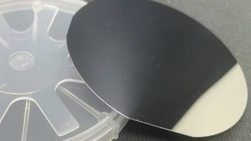
The stress issue:
GaN and its substrates have significantly different coefficients of thermal expansion (CTE):
| Material | CTE (×10⁻⁶/K) | Lattice Mismatch to GaN |
|---|---|---|
| GaN | 5.6 | 0% |
| Sapphire | 7.5 | 13.5% |
| Silicon | 2.6 | 17% |
| SiC | 4.2 | 3.5% |
This CTE mismatch leads to:
Residual stress in the epitaxial layer stack during cool-down from growth temperatures (typically > 1000°C)
Wafer bow (especially for GaN-on-Si) that complicates alignment and focusing
Stress concentration at the cleavage plane during dicing
Layer delamination at the heterointerface when mechanical force is applied
Additional challenges specific to GaN-on-sapphire:
Sapphire has Mohs hardness of 9, comparable to SiC, causing blade wear issues.
Sapphire is transparent, requiring special optical considerations for laser processing.
Typical die sizes for micro-LEDs are extremely small (10–100 μm), demanding ultra-narrow streets.
For GaN-on-silicon:
Silicon is absorbing at 1064 nm, requiring careful depth control to avoid substrate damage.
The large CTE mismatch leads to significant wafer bow (often > 100 μm for 150 mm wafers).
Mixed-material stack (GaN + Si) complicates laser parameter selection.
For micro-LED applications where die sizes approach 10–20 μm, the kerf width becomes a dominant yield factor. At 5 μm kerf (picosecond), streets can be as narrow as 10 μm, vs. 30–40 μm streets required for blade dicing — potentially doubling or tripling the number of dies per wafer.
The heteroepitaxial structure of GaN wafers presents unique optical and mechanical challenges that require sophisticated laser dicing strategies.
Challenges across GaN-on-Sapphire:
Sapphire absorbs minimally at 1064 nm, allowing the beam to penetrate deep into the substrate. This means the focal position must be precisely controlled to avoid heat accumulation at the GaN-sapphire interface, which could induce delamination.
The high bandgap of GaN (3.4 eV) means its absorption at 1064 nm is nonlinear — requiring high peak intensities to achieve ablation, which the picosecond pulse delivers perfectly.
Challenges across GaN-on-Silicon:
Silicon strongly absorbs 1064 nm, meaning most of the laser energy is deposited in the silicon substrate. For stealth dicing, the focus must be precisely positioned within the silicon substrate (not at the GaN-Si interface) to create a cleavage plane.
The 150–200 μm wafer bow typical of GaN-on-Si requires dynamic focus tracking to maintain consistent focal depth from wafer center to edge.
The picosecond solution for both:
For GaN-on-sapphire: The picosecond pulse passes through the transparent sapphire with minimal energy deposition, then ablates the GaN layer through nonlinear absorption, and finally modifies the sapphire through multi-photon processes. This sequential "depth-optimized" ablation creates a clean vertical sidewall through the entire material stack.
For GaN-on-silicon: Stealth dicing is the optimal approach. The picosecond pulse focuses within the silicon substrate (~50 μm below the GaN-Si interface), creating a modified layer. The tensile stress in the GaN layer (due to CTE mismatch) actually aids separation during tape expansion, resulting in exceptionally clean sidewalls.
Critical process control: The low fracture toughness of GaN (similar to SiC) demands minimal thermal stress. The picosecond pulse's cold ablation mechanism ensures temperature rise at the GaN layer remains below 100°C, preserving the delicate heterointerface.
For GaN-on-silicon, GaN-on-sapphire, and increasingly GaN-on-SiC wafers, achieving micro-crack-free dicing demands a laser platform that can handle complex material stacks with varying absorption properties, CTEs, and fracture toughness. This is not a problem that generic laser systems can solve.
Chanxan Laser's Picosecond Laser Wafer Dicing Machine is specifically engineered to meet the ultra-fine tolerances demanded by GaN device manufacturing. Whether you are dicing 100 μm GaN-on-sapphire for micro-LEDs or 500 μm GaN-on-Si for power devices, our system delivers the precision and yield required for commercial production.
Advance your semiconductor manufacturing efficiency with Chanxan Laser precision.
Inquire our engineers for a free sample dicing test today →| Free solution
Previous: Precision Laser Dicing for Glass Wafers and TGV Substrates
Next: Laser Dicing Solutions for SiC Wafers: Overcoming High Hardness & Thermal Stress