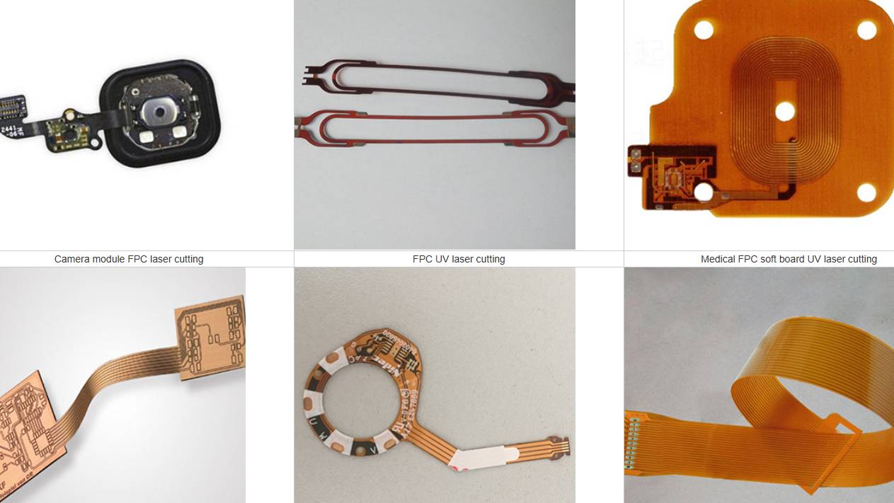
Flexible printed circuit boards (FPCs) have become an essential foundation of modern electronics, enabling lighter, thinner, and more compact product designs. From smartphones and wearable devices to automotive electronics, medical equipment, and aerospace systems, flexible PCBs provide design freedom that conventional rigid boards cannot achieve.
What Is a Flexible PCB?
A Flexible Printed Circuit Board (FPC), also known as a flex PCB, is a printed circuit built on a flexible insulating substrate instead of a rigid fiberglass laminate. The flexibility of the substrate allows the circuit to bend, fold, or twist repeatedly while maintaining stable electrical performance.
Compared with rigid PCBs, flexible circuits offer several advantages:
Reduced weight and overall device thickness
Excellent bending and dynamic flex performance
Higher wiring density in compact spaces
Improved assembly efficiency
Fewer connectors and solder joints
Greater design freedom for complex profiles
Understanding the Flexible PCB Structure
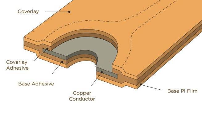
Although flexible PCBs appear simple, they consist of multiple engineered layers designed to balance electrical conductivity, insulation, flexibility, and mechanical protection.
Typical single-sided FPC construction includes:
Coverlay (Protective insulation film)
Copper foil (Conductive traces)
Adhesive layer (Optional or standard)
Polyimide (PI) film (Base substrate)
Note: For double-sided or multilayer FPCs, additional copper circuits, bonding layers, and reinforcement materials are incorporated based on layout complexity.
Polyimide (PI) Film: Polyimide acts as the primary substrate material for flexible PCBs. Thanks to its excellent flexibility, high dielectric strength, premium thermal stability, and chemical resistance, PI film remains the definitive base substrate choice for high-performance flexible electronics.
Copper Foil: Forms the conductive pathways that transmit electrical signals. Depending on the application requirements, manufacturers select specific copper thicknesses to balance flexibility with current-carrying capability. High-density electronics often demand ultra-fine traces with strict dimensional tolerances.
Adhesive Layer: While traditional FPCs use generic adhesive layers to bond copper to PI, advanced micro-electronics manufacturing increasingly adopts adhesive-free laminates to achieve higher thermal resistance, reduced profile thickness, and better dimensional stability.
Coverlay: A protective insulation layer applied directly over the completed etched copper circuits. It provides robust electrical insulation and protects traces against environmental stressors during dynamic bending. Laser processing Solutions are commonly utilized to execute micro-precise openings in the coverlay for target solder pads and smooth component mounting.
Stiffeners (FR4 / Stainless Steel / PI): Selectively laminated onto engineered sections of an FPC (such as directly underneath terminal connectors) to provide mechanical reinforcement, support component insertion stress, and ensure secure structural assembly.
Flexible PCB Manufacturing Process Flow
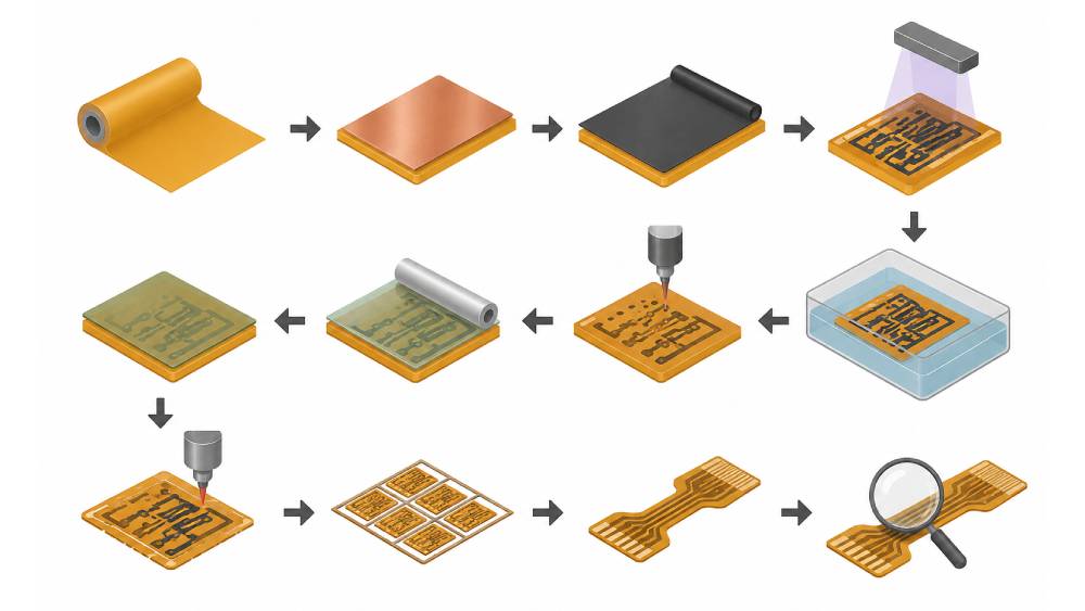
Although manufacturing methods scale depending on product layer counts and specifications, the overall fabrication workflow follows seven definitive structural stages:
1. Material Preparation
Production begins with selecting high-grade polyimide laminates and copper-clad materials. Raw material quality at this stage directly determines the baseline dimensional stability and long-term electrical reliability of the circuit panel.
2. Circuit Imaging and Exposure
A clean photoresist layer is laminated onto the raw copper surface. Using advanced photolithography, the specific high-resolution circuit pattern is exposed and transferred onto the target copper layer with high consistency.
3. Chemical Etching
Unwanted, non-circuit copper sections are chemically removed via precise etching solutions, leaving behind the fine conductive traces. As trace widths shrink to keep up with compact devices, etching accuracy demands undergo strict tolerances.
4. Hole Formation
Microvias and high-density through-holes are drilled into the board to establish secure interlayer electrical interconnections. Depending on target diameters, options include:
Conventional mechanical drilling
UV laser drilling systems
High-precision picosecond laser drilling
Advanced laser micro-drilling delivers distinct processing benefits for executing microscopic, ultra-fine vias with tight positional repeatability.
5. Coverlay Lamination
The prepared protective coverlay is carefully laminated directly over the completed etched circuits. Openings must align flawlessly with solder pads and surface component zones. Laser cutting serves as the premium choice here by removing physical tooling limits while yielding uniform edges.
6. Profile Cutting and Depaneling
Once structural processing wraps up, individual finished circuits are isolated and extracted from the main manufacturing panel. While mechanical routing or die matrix punching served legacy setups, modern complex geometries favor laser depaneling due to its superior edge quality and strict dimensional control.
7. Inspection and Testing
Each finalized batch undergoes comprehensive non-destructive quality evaluation:
Automated Optical Inspection (AOI)
Electrical continuity testing
High-resolution dimensional measurement
Visual cosmetic quality control
Where Laser Processing Delivers Significant Manufacturing Advantages
Traditional mechanical processing paths—like heavy die-cutting or mechanical routers—subject fragile, thin substrates to critical processing stress. Mechanical vibrations induce delamination, and physical blade wear creates jagged edge burrs. Modern non-contact laser processing has stepped in as the default industrial solution to resolve these bottlenecks across three major nodes:
Ⅰ. Microvia Drilling When via target diameters fall underneath 100 microns, mechanical bits break easily and struggle with high taper ratios. UV and Ultrafast lasers excel at executing blind and through-vias down to micron dimensions while maintaining excellent circularity, flawless positioning, and virtually zero thermal stress to embedded internal copper plates.
Ⅱ. Coverlay Window Opening Ablating tiny, precise window openings over micro-solder pads demands extreme accuracy. Laser cutting skips high tooling setup costs and long lead times of mechanical stamps, vaporizing cleanly directly via CAD vectors without pulling, wrinkling, or lifting thin insulating films.
Ⅲ. Profile Cutting and Depaneling Isolating dense, custom-shaped FPC panels represents a high-risk operation. Laser singulation applies completely zero mechanical load on internal traces, yielding burr-free and mechanical stress-free profiles. This eliminates micro-fracturing or crack spreading inside fragile joints sitting near cut boundaries.
Why Picosecond Lasers Are the Preferred Choice for Advanced FPC Production
When filtering for the best laser setup, the pulse duration is what dictates the final edge processing quality. Legacy thermal-based CO₂ lasers clear out materials using photothermal melting, which inevitably transmits an expansive Heat-Affected Zone (HAZ), deformed melted borders, and undesirable edge carbonization (charring) on thin polyimide.
In stark contrast, Picosecond Lasers deliver ultra-short laser bursts, utilizing professional "cold ablation" processing. The pulse width is brief enough to complete processing before thermal conduction can spread, cleaving raw molecular bonds instantly instead of heating up neighboring functional components.
Key Performance Benefits of Picosecond Laser Systems:
Near-Zero Heat-Affected Zone (HAZ): Safely prevents peeling or delamination across thin copper-PI boundary layers.
Carbonization-Free Edges: Avoids residue charring, guaranteeing complete, clean electrical insulation paths right along cut borders.
High Dimensional Tolerances: Capable of mapping microscopic profiles, ultra-fine traces, and micro-radius corners with total consistency.
Toolless Operational Flexibility: Drastically slashes upfront tooling costs while enabling instant prototyping for agile high-volume, high-mix runs.

Conclusion: The New Industry Standard
The ultimate electrical and mechanical performance of a flexible circuit depends entirely on the precision achieved during its fabrication. As next-generation electronics continue to push toward tighter tolerances, thinner profiles, and finer pitch constraints, traditional mechanical manufacturing methods have definitively reached their physical limits.
Integrating picosecond laser technology into the FPC production workflow is no longer just an optional competitive upgrade—it has rapidly evolved into the global industry standard for manufacturers seeking to boost product reliability, increase automation, and maximize yield.
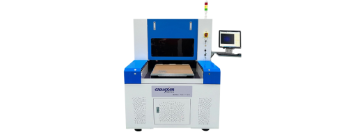
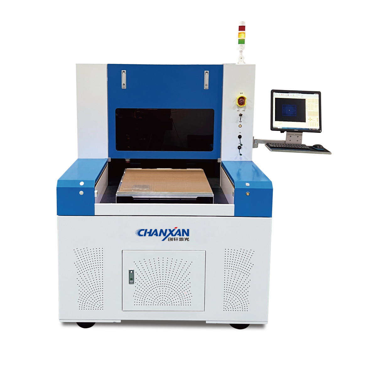
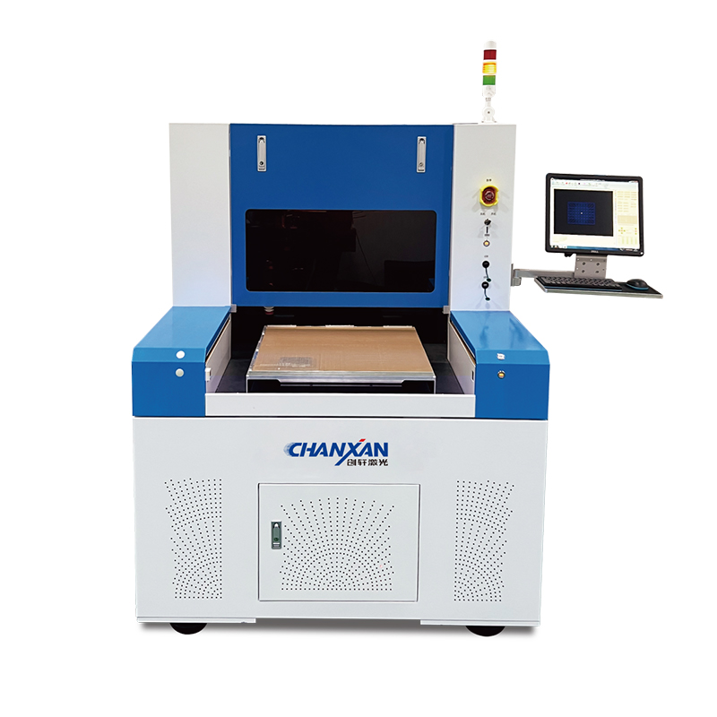
Featured Solution: Chanxan Precision Picosecond Laser Systems
To satisfy these rigorous micro-electronics processing demands, Chanxan Laser offers a specialized lineup of high-precision ultrafast laser equipment purposely engineered for next-generation FPC manufacturing. Balancing extreme optical path precision with high-volume production throughput, Chanxan's picosecond laser systems supply the definitive answer to complex advanced micro-machining bottlenecks:
Ultra-Short Pulse Ablation: Utilizes advanced picosecond technology to achieve ideal "cold processing," vaporizing target molecular zones instantly without giving heat time to conduct into sensitive traces.
Microscopic Heat-Affected Zone (HAZ): Restricts the total thermal impact zone down to a microscopic ≤ 3μm layer, fully shielding panels against edge yellowing, carbon charring, and delamination risks.
Industrial-Grade Rigidity & Stability: Built on a heavy-duty, high-stability minimalist framework paired with premium optical path configurations, ensuring sub-micron positioning repeatability across continuous, high-speed automated factory shifts.