Key Words: Silicon Wafer Dicing PCB Depaneling Glass Cutting
Home > News > Industry News
【Description】:
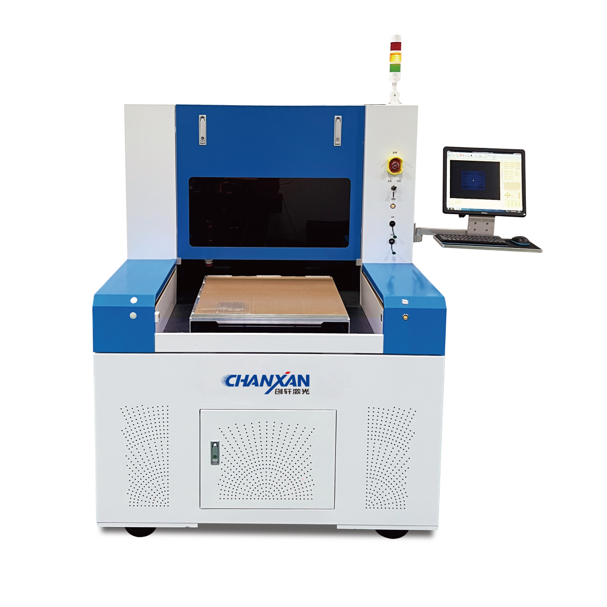
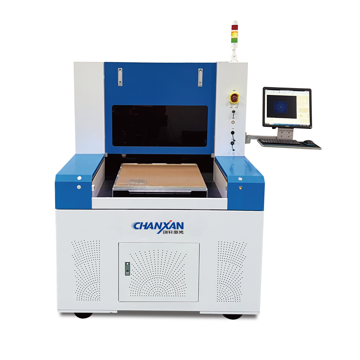
Eliminate chipping & micro-cracks with the Chanxan CW-6050PZ picosecond wafer dicing machine. Achieve a <3μm HAZ & narrow scribe streets for silicon, SiC & glass.
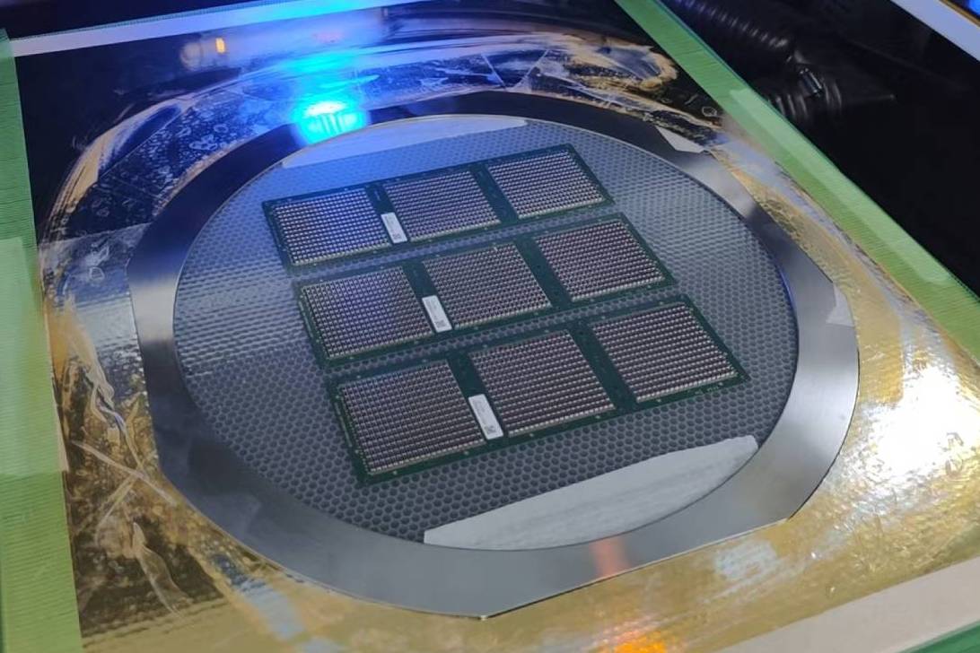
Silicon wafers remain the absolute backbone of the semiconductor industry, powering everything from high-density memory chips to advanced logic processors and power management ICs. However, as next-generation devices trend toward ultra-thin die profiles (50–100 μm) and narrower street widths (30–50 μm), conventional singulation processes have become critical yield bottlenecks.
Severe Chipping: Edge chipping up to 20–30 μm on front surfaces and extensive backside chipping that compromises die reliability.
Latent Material Defects: Micro-cracks propagating beneath the surface, leading to unpredictable field failures in stacked die packages and automotive ICs.
High Kerf Loss: Wide cutting streets of 25–40 μm drastically reduce the net number of usable dies per wafer.
Contamination Risks: Heavy reliance on coolants introduces particulate contamination, mandating aggressive post-dicing cleaning phases.
To achieve zero-stress singulation, the transition from nanosecond thermal processing to ultra-short-pulse picosecond dicing is essential. Nanosecond lasers operate in a thermal regime where pulse durations exceed the electron-phonon coupling time of silicon (~1–10 ps), causing heat diffusion, melt pools, and a 10–15 μm heat-affected zone (HAZ).
Chanxan's picosecond laser dicing systems operate exclusively in the "cold ablation" regime. By delivering peak intensities exceeding 10¹² W/cm² within a 1–10 ps pulse width, the system drives multi-photon absorption and avalanche ionization:
Instantaneous Bond Shattering: Breaks atomic bonds of silicon before heat can transfer to the surrounding crystal lattice.
Debris-Free Plasma Ejection: Material is directly ejected as ionized plasma rather than molten droplets, avoiding residual tensile stress.
Sub-3μm HAZ: Confines thermal diffusion to less than 3 μm, easily fitting within the tightest scribe street allocations.
Engineered for high-volume semiconductor environments, the CW-6050PZ delivers stable precision verified under production conditions:
| Performance Parameters | Specification Metric (CW-6050PZ) |
|---|---|
| Laser Source Type | Picosecond UV / IR / Green (Stability Optimized) |
| Laser Rated Power | 30W |
| Transmission / Motion Axis | X/Y/Z Three-Axis Air-Bearing Motion Stage |
| Working Area Options | 500mm * 500mm / 600mm * 900mm |
| Custom Adsorption Platform | 1200mm * 700mm (Highly Customizable) |
| Max Machining Thickness | ≤ 3.0 mm (Multi-pass scanning configuration) |
| Maximum Processing Speed | ≤ 3000 mm/s |
| Overall Machining Accuracy | ≤ 30 μm |
| Positioning & Repeatability | ±1 μm (Nanometer-level feedback loops) |
| Software & Supported Formats | Chanxan Self-developed Controls (PLT, DXF, DWG, AI, LAS, etc.) |
| Physical System Dimensions | 2100mm * 1550mm * 1750mm (380V ±10%, 50HZ) |
To satisfy the extreme metrics required by advanced fabs—ranging from 5nm logic chips to complex 200+ layer 3D NAND architecture—Chanxan integrates automated wafer loading/unloading frameworks alongside custom optics. Our system guarantees perfect kerf quality not just for silicon, but also for advanced silicon carbide (SiC) and ultrathin glass wafers.
Send us your silicon wafer specifications or design files to experience the ultra-clean edges and zero-stress singulation of Chanxan picosecond dicing technology.
Q: Can picosecond laser dicing handle thick power device wafers up to 750 μm?
A: Yes. For thicker wafers, we employ a multi-pass scanning strategy paired with dynamic focus management. Each high-speed pass cuts 30–50 μm layers with zero edge degradation, making it highly profitable for high-value power electronics.
Q: What is the absolute minimum scribe street width achievable?
A: With our tightly focused spot resulting in a 5–8 μm kerf and an alignment precision of ±1 μm, street widths can be narrowed down to 10–15 μm. This delivers an immediate 15–20% increase in net die yield per 300mm wafer.
Q: Does the system require special wafer handling or custom dicing tape?
A: No, standard UV-curable dicing tapes are completely compatible. Because our picosecond ablation induces near-zero mechanical shock, backside stress is eliminated, allowing some fabs to process wafers under 200 μm entirely without tape.
| Free solution