Key Words: Silicon Wafer Dicing PCB Depaneling Glass Cutting
Home > News > Industry News
【Description】:
Explore advanced picosecond laser dicing solutions for silicon carbide (SiC) wafers. Resolve high hardness & mechanical blade dicing limitations.
Silicon carbide (SiC) has emerged as the transformative material for next-generation power electronics, offering:
• 10× higher breakdown field than silicon • 3× wider bandgap enabling higher temperature operation (up to 600°C) • 3× higher thermal conductivity for superior heat dissipation • Higher switching frequency for more compact, efficient power modules
But these same properties that make SiC electrically superior also make it exceptionally difficult to process. With a Mohs hardness of 9.5 (approaching diamond at 10), SiC is one of the hardest known materials used in semiconductor manufacturing.
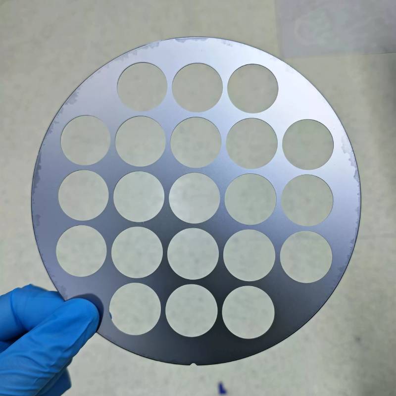
Rapid blade wear: Diamond-impregnated blades wear 5–10× faster on SiC than on silicon.
Extended cutting time: Each pass is painfully slow (1–2 mm/s) with 15–20 passes required for 350 μm wafers.
High mechanical stress: Cracking and edge delamination are common, particularly near the wafer edge.
Tooling cost: Blade replacement and dressing add significant cost of ownership.
Kerf loss: Wide 80–100 μm kerf translates to substantial loss of valuable SiC area.
For a material where a 150 mm SiC wafer can cost $2,000–$3,000, the yield loss from dicing defects and material waste has direct economic impact. The industry imperative: Transition from mechanical cutting to advanced laser solutions that preserve SiC's structural integrity while enabling economical processing.
| Parameter | Mechanical Blade Dicing (SiC) | Nanosecond Laser Dicing | Picosecond Laser (Stealth) Dicing | Picosecond (Ablation) |
|---|---|---|---|---|
| Cutting Speed | 1–2 mm/s | 5–10 mm/s | 50–100 mm/s | 100–300 mm/s |
| Kerf Width | 80–120 μm | 30–50 μm | N/A (stealth) | 8–15 μm |
| Material Removal | Mechanical grinding | Thermal ablation | Bulk modification | Cold ablation |
| Edge Chipping | 15–30 μm | 5–10 μm | < 1 μm (stealth) | < 2 μm |
| Heat-Affected Zone | N/A | 15–20 μm | < 1 μm | < 3 μm |
| Surface Contamination | Slurry/debris | Sputtered debris | None (stealth) | Minimal |
Industry Trend: Stealth dicing (internal bulk modification) is preferred for SiC because it offers zero kerf loss and exceptional edge quality. However, for applications requiring full isolation (such as power device singulation with thick metal layers) or for wafers where stealth dicing is not feasible, ablation-based picosecond dicing provides superior results to nanosecond alternatives.
The challenges in SiC processing stem from its unique material properties:
| Property | SiC (4H) | Silicon | GaN |
|---|---|---|---|
| Mohs Hardness | 9.5 | 7 | 8 |
| Fracture Toughness (MPa·m¹/2) | 3.0 | 0.95 | ~1.5 |
| Thermal Conductivity (W/m·K) | 370 | 150 | 230 |
| Bandgap (eV) | 3.26 | 1.12 | 3.4 |
| Debye Temperature (K) | 1200 | 645 | ~800 |
SiC's high Debye temperature and low fracture toughness mean that:
• Heat accumulation is dangerous: Localized heating creates thermal stress gradients that exceed the material's low fracture toughness, inducing cracks. • Mechanical force is inefficient: The high hardness requires immense force, but the low toughness means the material cracks rather than plastically deforms. • Thermal conductivity works against fast lasers: While beneficial for device operation, high thermal conductivity means heat spreads rapidly during laser processing, enlarging the HAZ.
Ultrashort pulse (picosecond/femtosecond) ablation addresses these challenges through:
• Nonlinear absorption: SiC is transparent at 1064 nm, but the peak intensity of a picosecond pulse (> 10¹² W/cm²) drives multi-photon absorption localized to the focal volume, confining energy deposition to less than 1 μm³. • Cold ablation: Material is removed through sublimation/ionization before heat diffuses from the focal volume, effectively "de-coupling" energy deposition from thermal transport. • Single-pass capability: High repetition rate (400 kHz–1 MHz) enables rapid material removal without cumulative heating — each pulse acts on fresh material.
Wafer orientation matters: C-axis (0001) orientation vs. off-axis affects propagation of stealth-modified layers.
Metal layer compatibility: For devices with thick Cu/Ni metallization on the front-side, ablation mode may be required to cut through the metal, followed by stealth dicing through the substrate.
Thick wafer handling: For 500–700 μm wafers, multiple stealth passes at different depths (2–3 passes) with varying pulse energies achieve clean separation.
Eliminating the micro-cracks, delamination, and low throughput of mechanical SiC dicing requires a fundamental rethinking of process physics. Standard nanosecond lasers introduce thermal stress that is incompatible with SiC's low fracture toughness. The industry is rapidly transitioning to picosecond-based solutions.
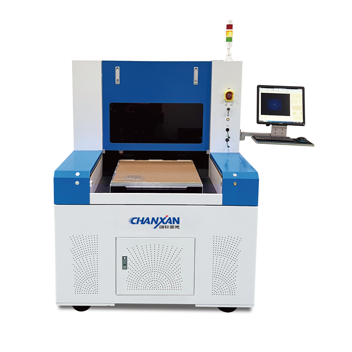
Chanxan Laser's Picosecond Laser Wafer Dicing Machine is specifically engineered to meet the ultra-fine tolerances demanded by SiC power devices.
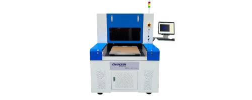
Send us your SiC wafer specifications or design files to experience the ultra-clean edges and high throughput of Chanxan picosecond dicing technology.
Q: Which is better for SiC — stealth dicing or ablation dicing?
A: The choice depends on your application. Stealth dicing offers zero kerf loss and the highest throughput, making it optimal for SiC power devices where every square millimeter of expensive SiC is valuable. However, ablation dicing is preferred when: (1) the device has thick front-side metallization (e.g., > 5 μm Cu), (2) the wafer has significant bow, or (3) the die design requires complete isolation cut for sidewall passivation.
Q: How does SiC laser dicing compare in cost of ownership vs. blade dicing?
A: While the initial capital investment for a picosecond laser dicing system is higher than a blade dicing tool, the total cost of ownership (TCO) is substantially lower: blade costs for SiC are extremely high (blades last only 100–200 cuts), throughput is 5–10× lower, and yield loss from chipping/cracking is significantly higher. Most SiC fabs achieve payback on a picosecond system within 12–18 months based on reduced tooling costs and improved yield alone.
| Free solution
Previous: Precision Laser Dicing for GaN-on-Silicon and GaN-on-Sapphire Wafers
Next: How to Minimize Edge Chipping in Silicon Wafer Laser Dicing?