Key Words: Silicon Wafer Dicing PCB Depaneling Glass Cutting
Home > News > Industry News
【Description】:
Comprehensive comparison between laser cutting and mechanical die cutting for thin film components including Polyimide (PI/Kapton), PET, and flexible printed circuits.
When manufacturing thin film components—such as Polyimide (PI/Kapton), PET, coverlays, and protective films—engineers and procurement managers frequently encounter a critical decision: "Should I use laser cutting or die cutting?"
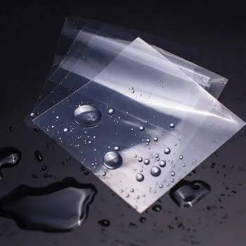
Die cutting is a traditional mechanical cutting process that uses a physical custom tool—a steel rule die or rotary die—to stamp or punch physical shapes out of thin film substrates.
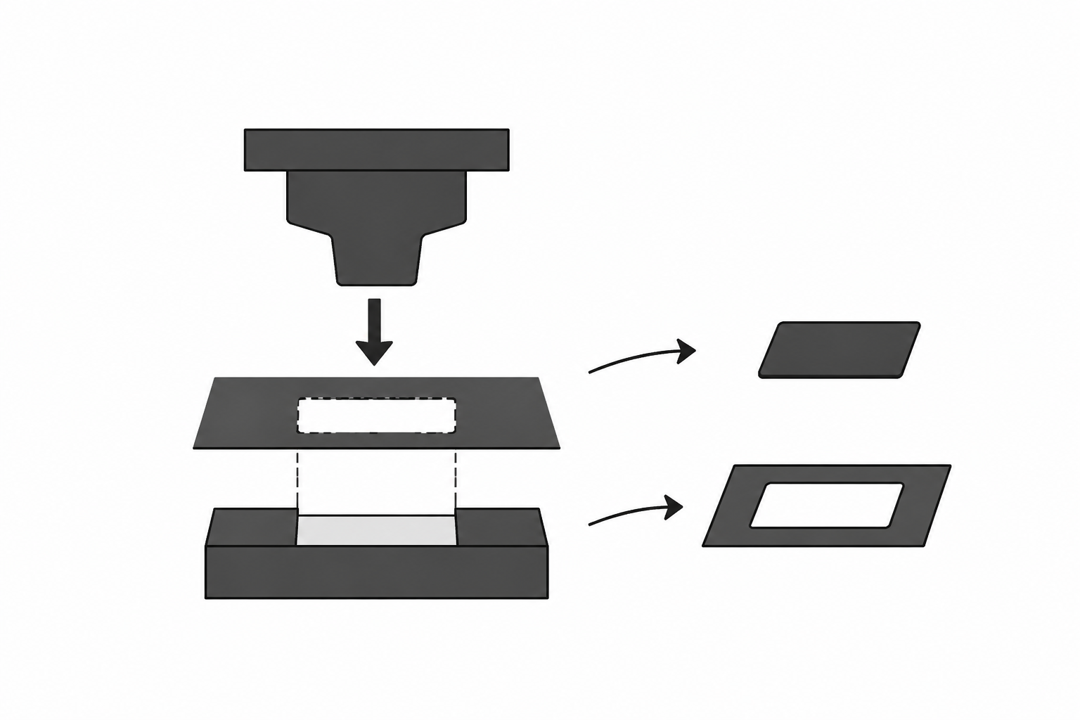
High Processing Speed: Once set up, mechanical dies stamp parts at high cycle speeds, making them efficient for high-volume, low-complexity manufacturing.
Mature Technology: Mechanical die stamping is a standardized, well-understood manufacturing process with low operator entry barriers.
High Initial Tooling Costs: Every design modification requires fabricating a completely new physical die, driving up NRE (non-recurring engineering) fees.
Tooling Wear & Maintenance: Mechanical blades dull quickly when stamping tough thin films, causing edge burrs, micro-cracks, and material delamination that demand frequent blade replacements and line shutdowns.
Geometrical Limits: Mechanical die cutting cannot easily achieve tight radii, micro-vias, or tight-tolerance internal features without damaging thin films.
Laser cutting thin films is a non-contact, digital processing method that uses focused thermal or photo-ablative light energy to melt, burn, or vaporize thin film materials with high precision.
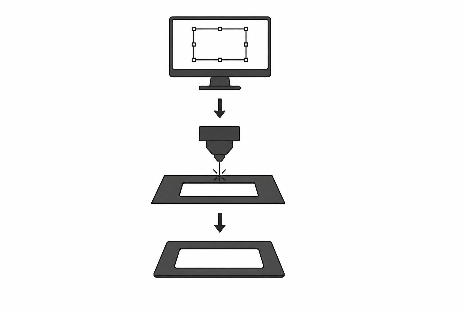
By eliminating physical contact, laser cutting allows concentrated photon energy to profile intricate geometry straight from CAD vector files, eliminating physical blades, mechanical stress, and mechanical tool wear entirely.
Comparing key parameters side-by-side demonstrates why high-precision sectors are transitioning to digital laser systems:
| Performance Parameter | Laser Cutting | Die Cutting |
|---|---|---|
| Tooling & Setup | No physical tooling (Direct CAD-to-part) | Physical dies required (Long lead time) |
| Complex Geometry | Excellent (Micro-features, sharp corners) | Limited (Constrained by blade radii) |
| Micro Hole Drilling | Excellent (Sub-50 micron micro-vias) | Poor (Prone to material tearing) |
| Design Flexibility | High (Instant digital modifications) | Low (Re-tooling needed for changes) |
| Edge Quality | Burr-free, stress-free | Potential burrs, stress cracks, and deformation |
| Prototyping Speed | Same-day iteration | Weeks for tool fabrication |
Selecting between laser cutting vs die cutting comes down to three primary factors:
Ultra-thin, rigid, or multi-layered flexible materials (such as Kapton, Polyimide, or copper-clad laminates) are sensitive to physical pressure. Die cutting can crush or delaminate sensitive films, whereas picosecond or UV lasers cleanly ablate material without mechanical force.
Low-to-Medium Volumes & Prototyping: Laser cutting is ideal because it requires zero tooling setup, allowing same-day turnaround for design revisions.
Ultra-High Volume Simple Shapes: Die cutting can offer lower per-part costs if the part shape is extremely basic and never changes.
If your tolerances are tight or your component contains intricate internal cutouts, micro-vias, or tight radii, laser cutting is often the only capable manufacturing process.
As consumer electronics, medical devices, and automotive electronics push for smaller form factors, traditional die cutting hits a physical wall. High-precision manufacturers are increasingly replacing mechanical die presses with ultra-short pulse picosecond and UV laser systems to achieve:
Minimal Heat-Affected Zone (HAZ): Advanced lasers cut thin films without carbonization or thermal damage.
Zero Mechanical Stress: Eliminates material warping, stretching, and edge burrs.
Maximum Yield: Digital vision alignment systems compensate for batch material distortion automatically, reducing scrap rates.
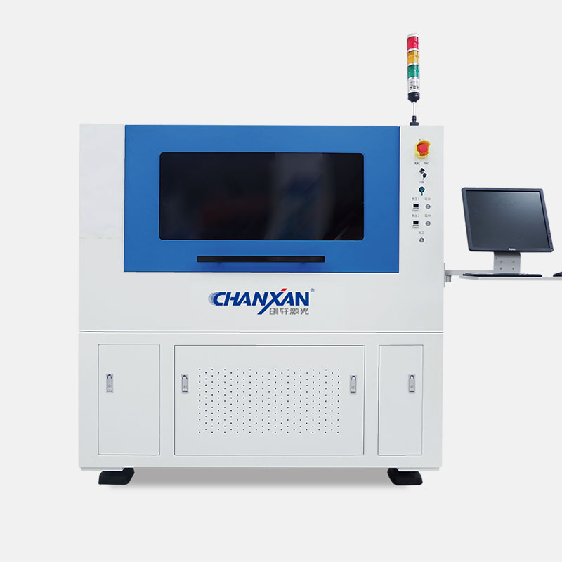
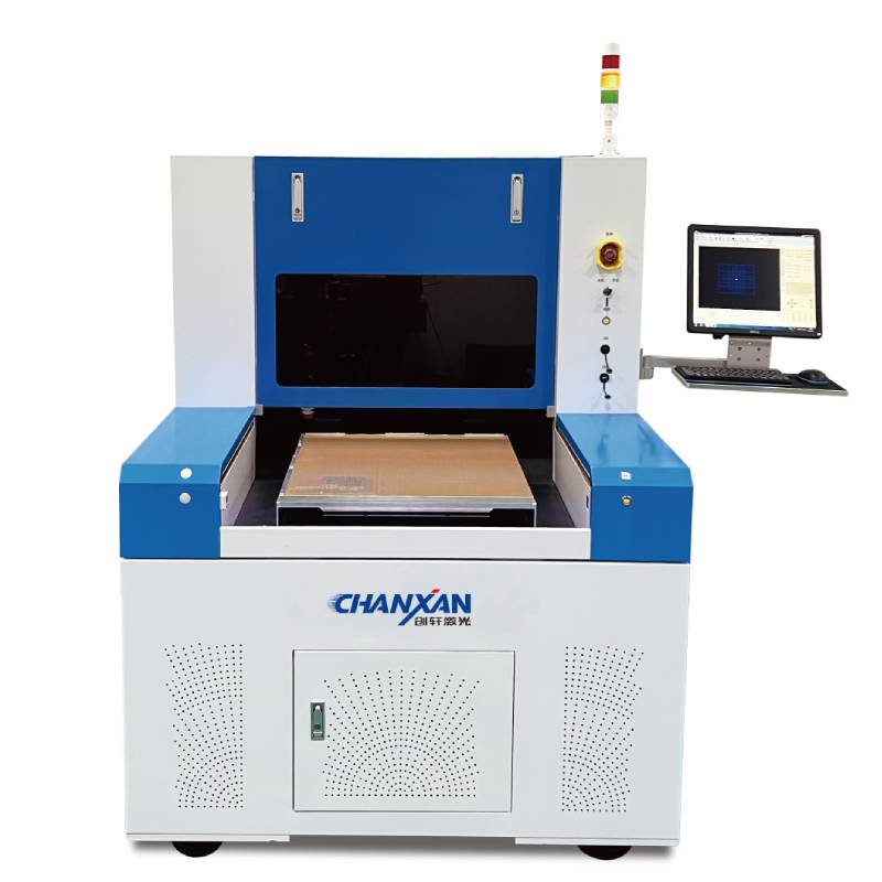
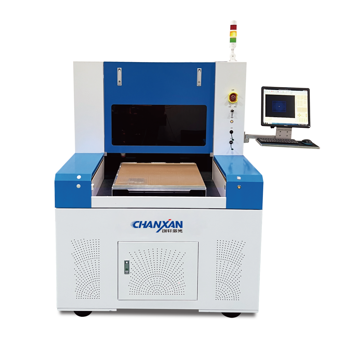
At Chanxan Laser, we engineer industrial ultrafast laser systems specifically designed for thin film, flexible printed circuit, and polyimide processing. Equipped with high-stability UV picosecond lasers, precision linear motor stages, and automatic CCD vision positioning, Chanxan laser cutting equipment ensures pristine edge quality, zero tool wear, and high throughput.
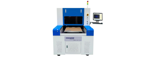
Whether you need to eliminate edge burrs on Kapton films or accelerate turnaround on micro-flex components, our engineering team is here to optimize your manufacturing workflow.
| Free solution
Previous: Introducing Chanxan 3D Five-Axis Laser Cutting Machine: Applications, Technology and Buying Guide
Next: High-Precision Polyimide Film Laser Cutting: The Ultimate Processing Solution for FPC Manufacturing