Key Words: Silicon Wafer Dicing PCB Depaneling Glass Cutting
Home > News > Industry News
【Description】:
Comprehensive guide to precision laser processing of functional thin films, covering ultrafast picosecond/femtosecond lasers, UV beam shaping, key industrial applications in flexible displays, semiconductors, and Chanxan Laser's ultrafast precision platform.
In high-end manufacturing fields such as semiconductor fabrication, next-generation energy storage, flexible displays, and microelectronics packaging, functional thin-film materials regularly operate at sub-micron and nanometer scales. Traditional mechanical cutting and long-pulse thermal processing methods often introduce structural issues like micro-cracking, severe heat-affected zones (HAZ), and film delamination. Precision laser processing of thin films has emerged as a critical non-contact, ultra-high-precision manufacturing technology that overcomes these physical limitations to enable next-generation micro- and nano-fabrication.
The efficiency and quality of precision laser processing depend directly on controlling the photon-matter interaction mechanism. Key technologies driving this field include:
Cold Processing Mechanism: Ultrashort pulse durations (femtosecond: 10-15 s, picosecond: 10-12 s) deliver peak energy before thermal diffusion occurs in the lattice network. Materials undergo direct plasma ablation without melting, eliminating heat-affected zones (HAZ) and edge burrs.
Nonlinear Absorption: High peak intensities allow transparent dielectrics and wide-bandgap thin films to absorb photon energy efficiently via multi-photon absorption.
Photochemical Cleavage: Ultraviolet (355 nm) and Deep-UV (266 nm or excimer) photons carry high single-photon energy capable of directly breaking chemical bonds in polymers and inorganic dielectrics. This minimizes thermal stress and produces fine, high-resolution features.
Top-Hat Beam Shaping: Refractive or diffractive optical elements (DOEs) convert standard Gaussian profiles into uniform top-hat intensity distributions, ensuring consistent laser fluence across the target surface and flat-bottomed ablative cuts.
Galvanometer & Motion Integration: Synchronizing high-speed Galvo scanners with linear air-bearing stages enables precise, dynamic laser patterning over large working areas.
| Sector | Film Material / Structure | Laser Processing Task | Performance Advantage |
|---|---|---|---|
| Flexible Displays (OLED / Micro-LED) | Polyimide (PI) substrates, ITO transparent conductive films, encapsulated thin films (TCE) | Laser Lift-Off (LLO), micro-patterning, dynamic film cutting | Zero thermal damage to sensitive underlying pixel circuits; sub-micron edge roughness. |
| Photovoltaics & Energy Storage | Perovskite thin films, silicon nitride (SiNx), lithium battery separator coatings | Selective P1/P2/P3 scribing, dielectric film removal | High selective ablation depth control (±10 nm); no collateral layer erosion. |
| Semiconductor & Microelectronics | Low-k dielectrics, metallic seed layers, redistributive layers (RDL) | Laser grooving, thin-film selective ablation, direct writing | Prevents chip delamination during dicing; supports ultra-dense micro-interconnects. |
| Medical & Consumer Electronics | Flexible Printed Circuits (FPC), optical coatings, sensors | Functional film micro-drilling, perimeter profiling, surface texturing | Clean cuts without carbonization; process flexibility without physical tooling wear. |
To transition ultrafast laser technologies from laboratory settings to continuous volume production, modern equipment architectures integrate several critical subsystems:
High-Stability Laser Sources: Industrial-grade ultrafast laser engines featuring high pulse repetition rates (kHz to MHz range) and active thermal stabilization ensure long-term power consistency (< 1% RMS).
Sub-Micron Motion & Positioning: Combining granite bases, linear motors, and air-bearing stages reduces high-frequency mechanical vibration. Closed-loop optical encoders provide sub-micron positioning accuracy (< 0.5 μm).
Machine Vision & Alignment Systems: High-magnification coaxial CCD cameras paired with Optical Coherence Tomography (OCT) allow automatic feature recognition, layer-depth measurement, and dynamic focus tracking across warped or uneven film surfaces.
Process Monitoring & Closed-Loop Control: Inline optical power sensors and optical emission spectroscopy continuously assess laser-material interactions to maintain dynamic depth control and immediately detect processing anomalies.
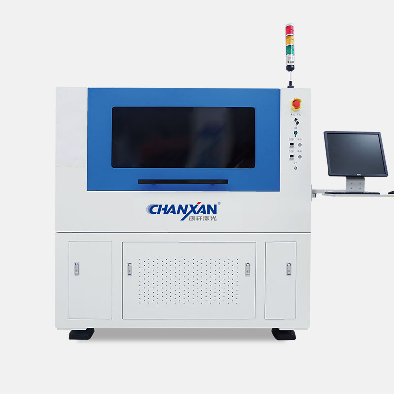
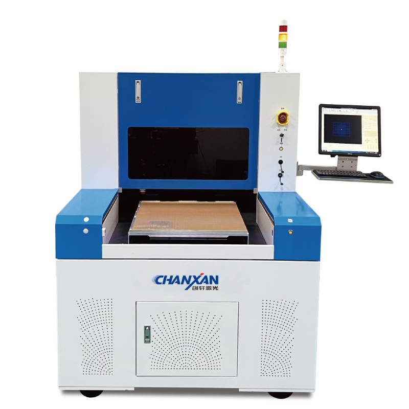
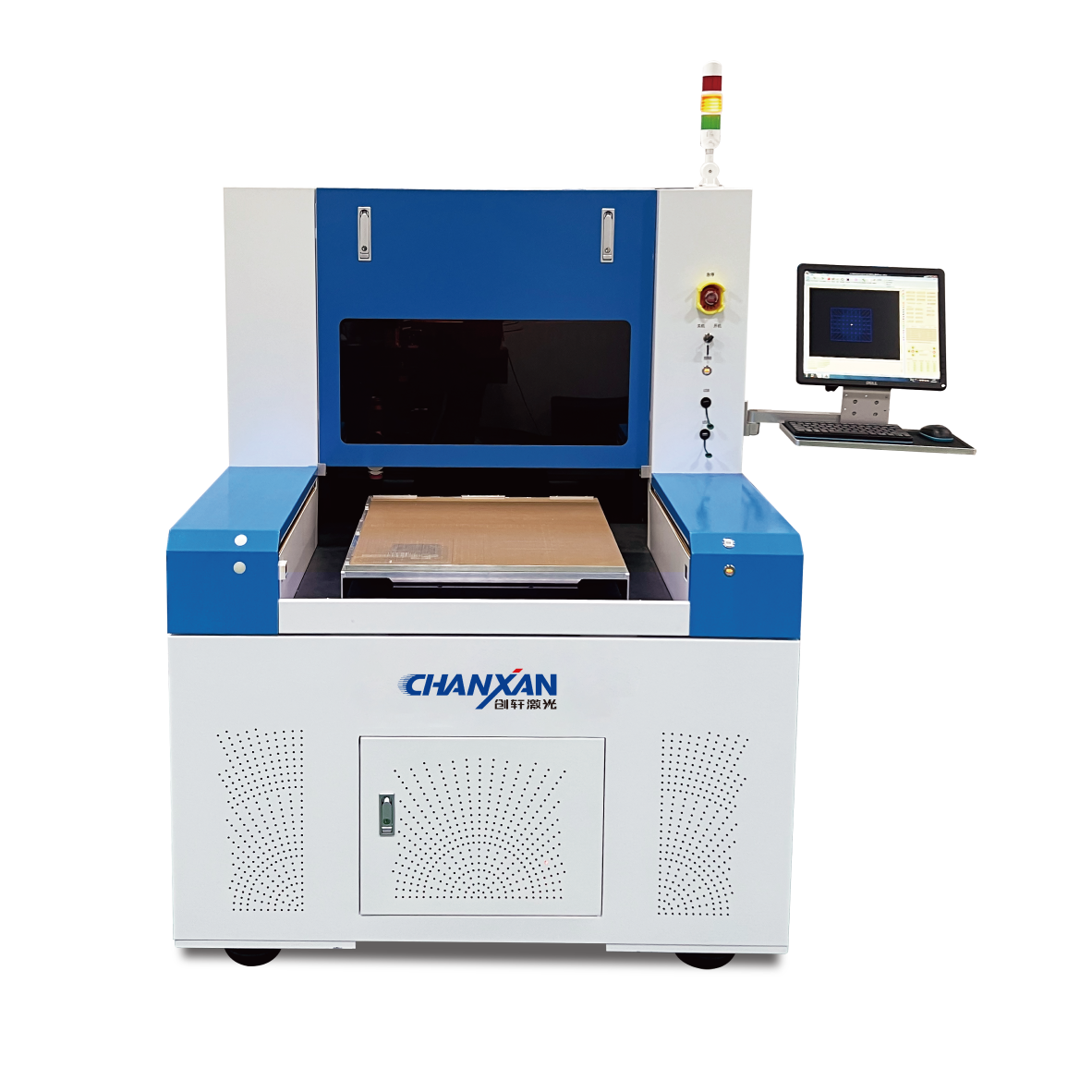
To bridge advanced photonic technology with demanding industrial manufacturing, Chanxan Laser has developed an integrated suite of ultrafast laser processing platforms engineered specifically for thin-film micro-fabrication, flexible electronics, and semiconductor-grade applications.

Ultra-Cold Processing & Zero Thermal Strain: Leveraging 355 nm ultraviolet picosecond and femtosecond laser configurations, Chanxan’s platform delivers pulse energy in sub-picosecond or picosecond regimes. By directly cleaving molecular bonds before heat propagates, the heat-affected zone (HAZ) is constrained within ≤ 5 μm, yielding burr-free, non-carbonized edges on sensitive PI films, FPC coverlays, and ITO/PET substrates.
Micron-Level Spot Focus & Motion Stability: Fitted with proprietary optical path control and high-precision focusing optics, the system produces focused beam spots as small as 3–5 μm. Supported by natural granite bed bases and linear-motor-driven X/Y air-bearing stages, it delivers sub-micron positioning accuracy for ultra-dense micro-hole arrays and ≤ 10 μm fine-line scribing.
Integrated Vision & Smart Automation: Featuring high-resolution coaxial CCD automatic vision alignment and dynamic galvanometer linkage, the system dynamically compensates for substrate warpage and material expansion. One-click CAD vector import enables rapid prototyping and continuous roll-to-sheet or sheet-to-sheet mass production across 3C electronics, semiconductor packaging, and new energy thin-film processing.
As device architectures transition toward smaller footprints and multi-layer 3D integration, precision laser processing of thin films will continue to evolve. Key ongoing developments include multi-beam parallel processing via spatial light modulators (SLM), adaptive optics for real-time focus correction, and machine learning-driven optimization of dynamic processing parameters. These innovations solidify laser-based film processing as an indispensable enabler for next-generation microelectronics, green energy, and advanced display technology.
| Free solution
Previous: Roll-to-Sheet Picosecond Laser Processing for Thin Film Manufacturing
Next: UV Picosecond Laser for OLED Processing – The Enabling Technology for Advanced Display Manufacturing