Key Words: Silicon Wafer Dicing PCB Depaneling Glass Cutting
Home > News > Industry News
【Description】:
Explore laser processing technologies in OLED manufacturing, including LLO, ELA, and UTG cutting. Discover Chanxan Laser's high-precision laser equipment solutions.
Driven by skyrocketing demand for lightweight, flexible, and high-refresh-rate displays in smartphones, wearables, automotive dashboards, and foldable devices, OLED (Organic Light-Emitting Diode) has cemented its position as the dominant technology in premium display manufacturing. As OLED panels transition from rigid glass substrates to flexible bases, notched geometries, and under-display cameras, industrial laser processing technology has become the core enabler of high-yield, high-precision production.
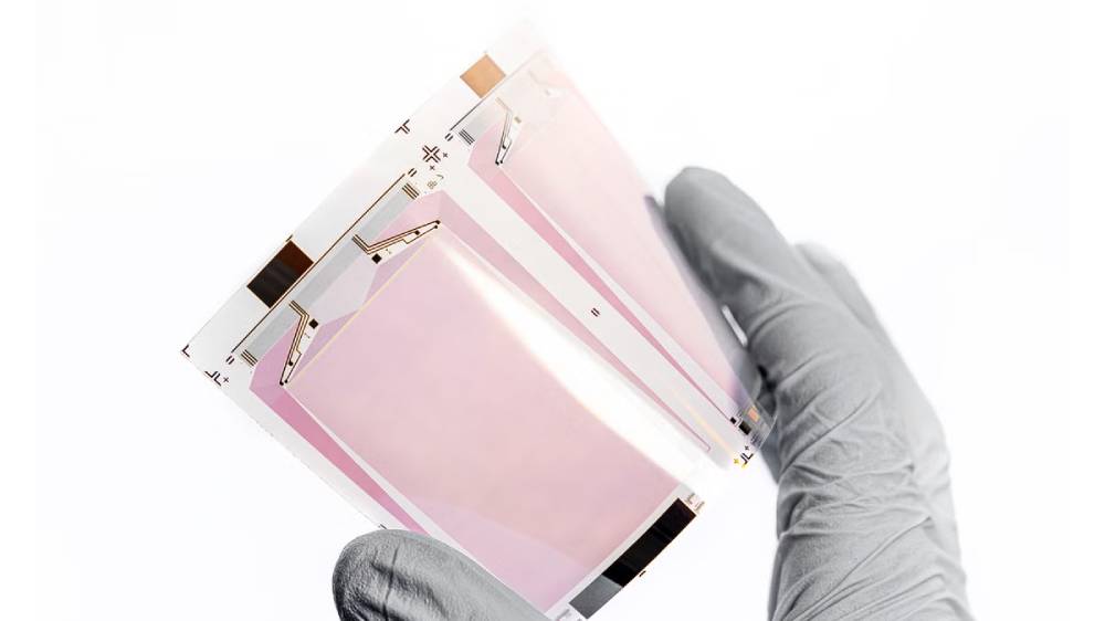
An OLED display panel comprises complex, multi-layered functional thin films with micron-level thickness, including organic light-emitting layers, metallic electrodes, flexible Polyimide (PI) substrates, encapsulation films, and Ultra-Thin Glass (UTG). Traditional mechanical cutting and chemical etching methods face severe physical limitations:
Thermal Degradation: Conventional thermal processing causes heat damage to delicate organic layers, leading to edge melting, delamination, and excessive Heat-Affected Zones (HAZ).
Mechanical Stress & Micro-Cracks: Physical blade cutting induces micro-cracks along cut edges, compromising panel bending fatigue life and lowering overall production yields.
Geometry Limitations: Mechanical tools cannot achieve sub-micron precision for complex shapes, such as camera hole punches (Hole-in-Active-Area), rounded corners, and freeform contours.
Non-contact laser processing addresses these challenges through high energy density, ultra-short pulse durations, and non-thermal "cold processing" mechanisms, making it an indispensable process in modern OLED fabrication lines.
| Laser Technology Type | Wavelength & Pulse Characteristics | Material Interaction Mechanism | Primary OLED Applications |
|---|---|---|---|
| UV / DUV Laser | Ultraviolet (248nm / 308nm / 355nm) | Photochemical ablation via direct molecular bond breaking | Laser Lift-Off (LLO), Excimer Laser Annealing (ELA) |
| Picosecond Ultra-Fast Laser | Pulse width in the 10-12s range | Low thermal diffusion, minimal heat transfer | Precision thin-film scribing, FMM micro-hole repair |
| Femtosecond Ultra-Fast Laser | Pulse width in the 10-15s range | Non-linear multiphoton absorption ("cold machining") | UTG cutting, bevel chamfering, defect repair |
Femtosecond and picosecond ultra-fast lasers deliver energy in ultrashort timeframes (Δt < 10-12s), shorter than the electron-phonon relaxation time of materials. Material vaporizes instantaneously through plasma formation before heat can diffuse, yielding extremely narrow kerfs, zero micro-cracks, and a Heat-Affected Zone (HAZ) of less than 3μm.
In large-area processes like Laser Lift-Off (LLO), diffractive optical elements (DOE) and flat-top beam shapers transform Gaussian laser beams into uniform line beams spanning hundreds of millimeters. This optics architecture ensures seamless intensity distribution across large display glass panels.
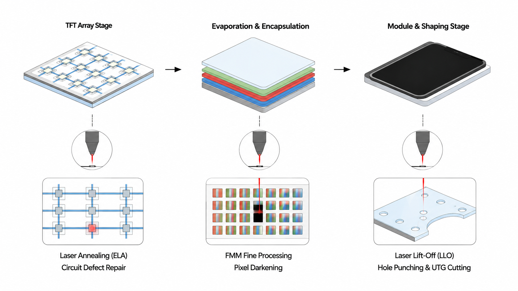
In flexible OLED production, ultra-thin Polyimide (PI) substrates cannot be processed standalone due to structural instability. PI is liquid-coated onto a rigid carrier glass substrate for array and evaporation steps. Once display fabrication is complete, a high-power UV laser beam passes through the transparent carrier glass, cleanly vaporizing the PI interface layer to separate the flexible display without applying mechanical stress.
Laser annealing transforms amorphous silicon (a-Si) thin films on the TFT substrate into low-temperature poly-silicon (LTPS). This structural phase change significantly boosts electron mobility, facilitating high-frequency pixel response for high-refresh-rate OLED panels.
Under-Display Hole Punching: Precise circular/oval micro-holes (C-Cup / U-Cup) are cut into the panel for under-display cameras and sensors without damaging surrounding active pixels.
Freeform Contour Dicing: Ultra-fast lasers execute smooth, chip-free dicing along curved notch edges, corner radii, and foldable display margins.
Ultra-Thin Glass (30μm ∼ 100μm thick) used in foldable screens requires extreme edge strength. Femtosecond lasers employ stealth dicing and laser-induced thermal stress splitting to create flawless cut edges without micro-fractures, maintaining maximum glass bending flexibility.
Post-encapsulation panels with short-circuits or point defects are inspected via high-magnification CCDs. Femtosecond laser pulses perform micro-circuit ablation, line disconnection, or pixel darkening, salvaging high-value display panels and increasing yield rates.
Deploying laser systems on high-throughput OLED production lines requires meeting rigorous industrial criteria:
Sub-Micron Motion & Positioning: Air-bearing motion stages driven by linear motors ensuring repeatable positioning within ±1μm.
Dynamic Vision & Auto-Focus Alignment: High-resolution CCD cameras capture Mark points, working alongside real-time distance sensors for dynamic focus tracking at ±0.5μm precision.
Debris & Contamination Control: High-efficiency differential vacuum extraction removes vaporized particulates, maintaining an optical cleanroom environment during laser ablation.
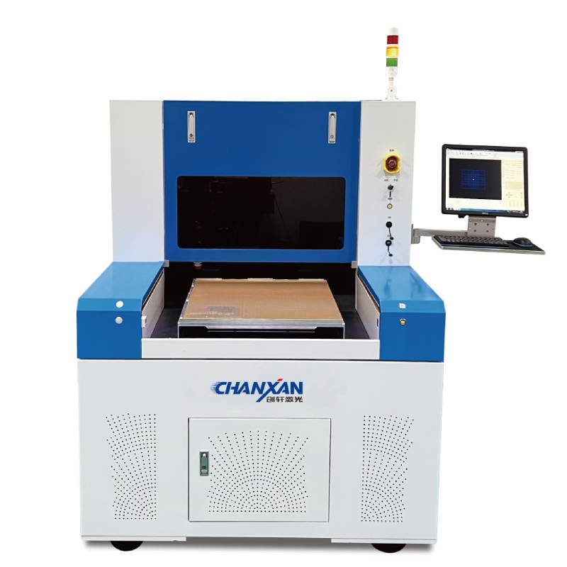
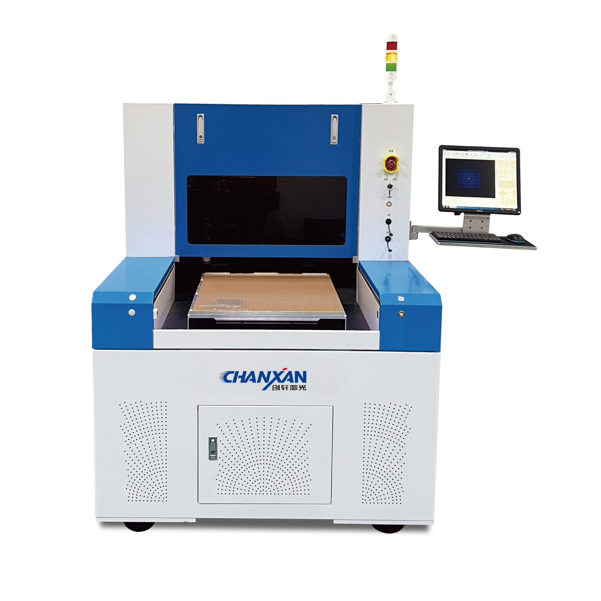
As an industry-leading manufacturer of high-precision industrial laser equipment, Chanxan Laser offers advanced ultra-fast laser processing systems tailored for microelectronics, semiconductor, and OLED display manufacturing.
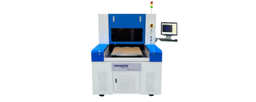
Ultra-Fast Cold Processing & Minimal HAZ Chanxan Laser's high-precision processing platforms integrate UV femtosecond and picosecond laser source technology. By maintaining a Heat-Affected Zone (HAZ) under 3μm, the equipment eliminates thermal edge degradation and micro-cracking across flexible films and brittle substrates.
Granite Motion Base & Air-Bearing Drive Built upon heavy-duty natural granite marble bases with precision air-bearing positioning systems, Chanxan laser machines effectively isolate environmental vibrations, ensuring long-term mechanical stability and sub-micron repeatability.
Integrated Vision & Intelligent Software Equipped with coaxially aligned high-resolution CCD optics and proprietary control software, Chanxan systems support automated CAD trajectory import, multi-focal depth compensation, and seamless integration into automated Industry 4.0 production lines.
Broad Micro-Machining Applications Beyond flexible OLED thin-film cutting, LLO assistance, and UTG dicing, Chanxan Laser equipment is widely deployed in semiconductor wafer scribing, FPC circuit drilling, ceramic dicing, and micro-medical device manufacturing.
As the global display industry continues to innovate, Chanxan Laser remains committed to empowering manufacturers with reliable, high-yield, and automated precision laser solutions.
| Free solution
Previous: Flexible OLED Laser Cutting – Precision Processing for Foldable and Rollable Displays
Next: Can Laser Cut Glass? The Complete Guide to Precision Glass Laser Cutting