Key Words: Silicon Wafer Dicing PCB Depaneling Glass Cutting
Home > News > Industry News
【Description】:
A comprehensive comparison between Laser Dicing and Plasma Dicing for advanced semiconductor wafer singulation. Explore principles, parameters, and applications for Si, SiC, and GaN.
As semiconductor devices become smaller, thinner, and more complex, traditional blade dicing faces increasing challenges such as chipping, cracks, and yield loss. Ultra-thin wafers, narrow dicing streets, and advanced materials like SiC and GaN are driving the adoption of alternative wafer singulation technologies.
Semiconductor wafer Laser Dicing and Plasma Dicing have emerged as two leading solutions. This article compares their working principles, advantages, limitations, and applications to help manufacturers choose the right technology for advanced semiconductor processing.
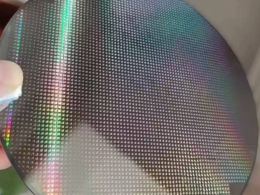
Laser wafer dicing is a highly versatile, non-contact singulation method that uses a tightly focused beam of light to separate dies. Depending on how the laser interacts with the material, the process generally falls into two categories: Laser Ablation and Stealth Dicing.
Older nanosecond lasers often left behind unacceptable heat-affected zones (HAZ) and recast material (debris). Modern, high-precision lines have transitioned to ultrafast lasers (picosecond and femtosecond pulse widths).
Because the laser pulse is incredibly short (measured in 10^{-12} to 10^{-15} seconds), the material transitions directly from a solid to a gas before heat has time to conduct into the surrounding substrate. This process, known as "cold processing", delivers three major benefits:
Minimal HAZ: The heat-affected zone is virtually non-existent (often under 3um).
Low Debris: Drastically reduces microscopic slag and dust, protecting sensitive surface circuits.
Ultra-Narrow Kerf: Enables cutting widths down to the single-micron level.
Plasma dicing (specifically, plasma etching wafer singulation) is a chemical and physical process that removes wafer material using reactive gas ions. It is fundamentally a dry etching process that borrows from established Deep Reactive Ion Etching (DRIE) technology.
Unlike laser dicing, which traces a beam sequentially along every street, plasma dicing is a batch process where the entire wafer is etched simultaneously.
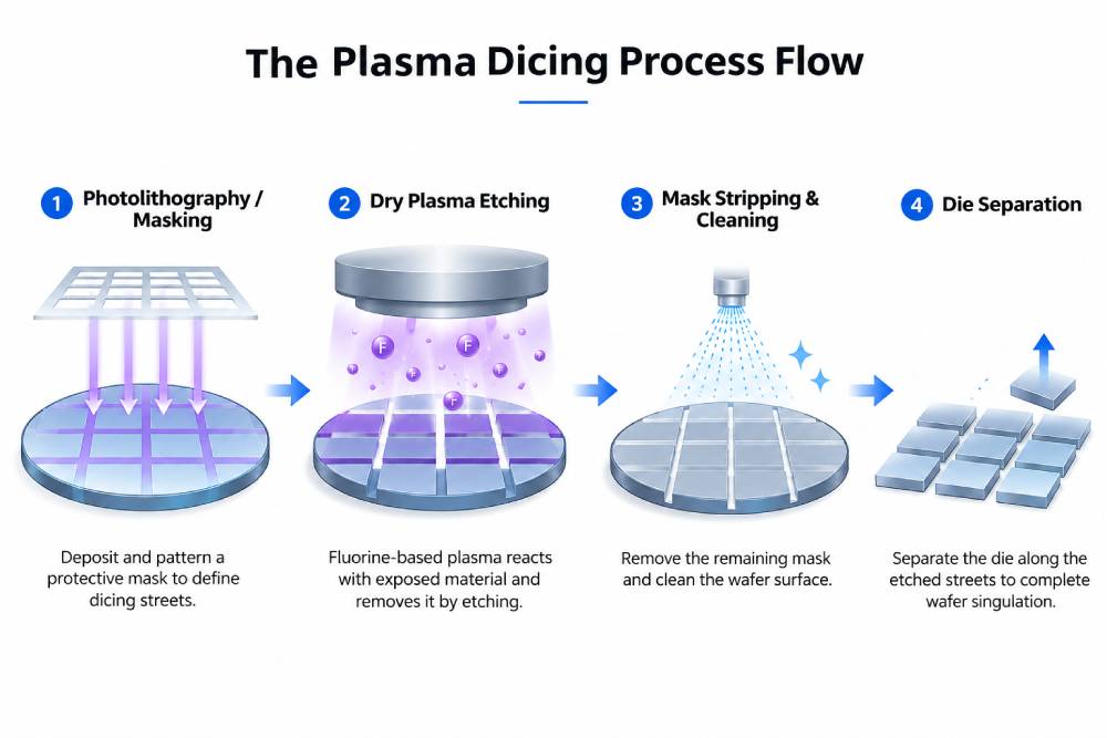
Masking: A protective photoresist mask or dicing tape is applied to the front of the wafer, leaving only the dicing streets exposed.
Plasma Etching: The wafer is placed in a vacuum chamber. Reactive plasma (typically fluorine-based chemistries for silicon) is generated. The ions chemically react with and physically bombard the exposed silicon, etching vertical trenches down to the dicing tape.
Singulation: The mask is stripped away, leaving clean, separated dies ready for pick-and-place.
| Parameter | Laser Dicing | Plasma Dicing |
|---|---|---|
| Process Mechanism | Laser ablation or internal modification | Plasma etching (chemical/physical DRIE) |
| Contact Type | Non-contact | Non-contact |
| Kerf Width | Narrow level (typically 5 - 15um) | Extremely narrow (can be < 5um) |
| Heat Affected Zone (HAZ) | Minimal to none (when using Ultrafast lasers) | Absolutely none |
| Throughput | High (sequential; speed depends on total path length) | Very High for small dies (batch process; independent of die count) |
| Mask Required? | No | Yes (adds lithography/coating and removal steps) |
| Material Flexibility | Excellent (Silicon, SiC, GaN, Glass, Ceramics) | Limited (Excellent for Silicon; highly complex for compound wafers) |
| Setup Complexity | Lower (Direct write from CAD file) | Higher (Requires cleanroom masking and etching steps) |
| Cost | Lower initial equipment investment | Higher capital equipment and running (gas/mask) costs |
Because ultrafast lasers can focus down to spot sizes of just a few microns, they allow for exceptionally narrow dicing streets. This saves valuable wafer real estate, allowing design engineers to pack more dies onto a single wafer and reduce overall material waste.
By utilizing picosecond and femtosecond laser pulses, the thermal interaction is tightly controlled. This avoids common thermal defects like:
Micro-cracks that can propagate during packaging or thermal cycling.
Melting and recast layers that interfere with subsequent assembly steps.
Delamination of fragile metal or low-k layers near the dicing street.
Perhaps the greatest advantage of laser systems is their material-agnostic nature. By tuning the laser's wavelength, pulse width, and power, a single laser tool can cut through Silicon, Silicon Carbide (SiC), Gallium Nitride (GaN), Glass, and Alumina Ceramics without needing entirely different chemistries or chamber setups.
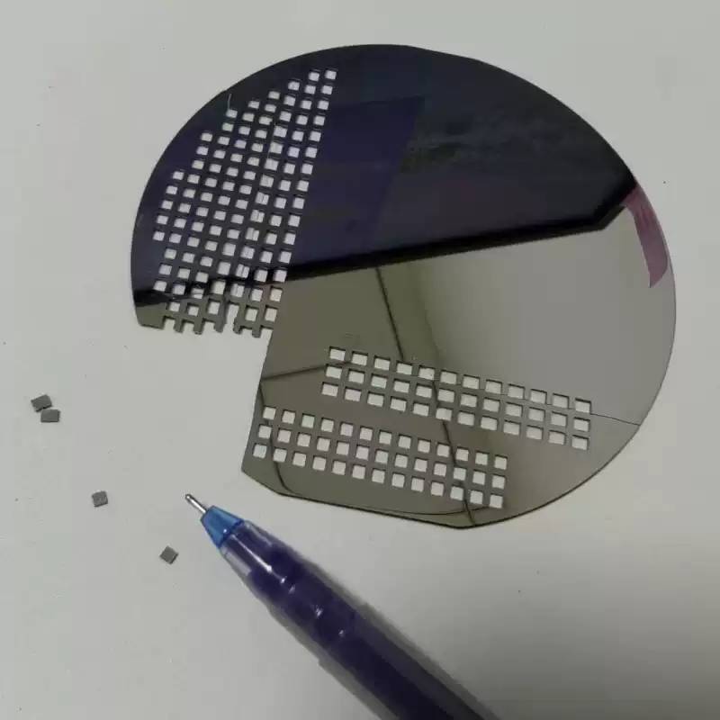
Because plasma dicing relies on anisotropic chemical etching rather than mechanical or thermal erosion, it can create incredibly thin dicing lanes (often under 5um), maximizing die count per wafer.
Because there is no physical force, heat, or shock wave applied to the crystal structure, plasma-diced chips exhibit up to twice the bending strength of mechanically cut chips. This is a game-changer for fragile, ultra-thin dies.
Because plasma dicing etches all streets at the exact same time, the throughput is completely independent of the number of cuts. If you are dicing a wafer into millions of tiny RFID chips or small-footprint sensors, plasma dicing is incredibly fast.
Choosing between these Laser Dicing vs. Plasma Dicing technologies depends on the wafer material you are processing:
Recommendation: Both are viable.
Selection Logic: For standard silicon wafers, laser dicing is highly favored for its flexibility and lower upfront cost. However, if you are handling ultra-thin silicon wafers (< 50um) with highly complex geometries or high volumes of microscopic dies, dry plasma dicing becomes highly attractive despite the masking overhead.
Recommendation: Ultrafast Laser Dicing
Selection Logic: Silicon Carbide (SiC) is extremely hard, brittle, and chemically inert. Plasma etching SiC is painfully slow and requires specialized, aggressive chemistries that wear down chambers quickly. Ultrafast lasers (especially picosecond systems) easily ablate or internally modify hard SiC crystal structures cleanly, making them the industry standard for EV and energy-infrastructure power chips.
Recommendation: Laser Dicing
Selection Logic: Gallium Nitride is typically grown on SiC or Sapphire substrates. This heterogeneous structure makes plasma dicing extremely difficult, as different layers require entirely different chemical etching rates. A tuned UV laser or ultrafast laser dicing setup handles these multi-material sandwiches with ease.
Recommendation: Both (Case-by-Case)
Selection Logic: MEMS devices have delicate moving microstructures on the surface. Laser dicing (especially stealth dicing) is excellent because it doesn't wash away or contaminate the structures. However, for complex MEMS designs where mechanical vibration of any kind must be avoided, dry plasma etching is preferred because it exerts zero mechanical load on the suspended structures.
Recommendation: Laser Dicing
Selection Logic: Laser cutting is the clear winner for glass. Ultrafast lasers can induce highly controlled internal modifications in glass substrates, allowing for clean, crack-free separation with optical-quality edge finishes.
If you are evaluating your next equipment investment, use this simplified decision framework to point you in the right direction:
| Key Requirement | Primary Driver | Recommended Technology |
|---|---|---|
| High Material Variety | Frequent changeovers between Si, Glass, SiC, GaN | Ultrafast Laser |
| Ultra-Thin Silicon (< 50um) | Maximum die strength and zero stress | Plasma Dicing / Laser |
| High Hardness (SiC/Sapphire) | Cutting hard, brittle compound semiconductors | Ultrafast Laser |
| Complex Non-Linear Cut Paths | Rounded, hexagonal, or irregular die shapes | Laser or Plasma (both support non-linear) |
| Low Capital Investment | Cost-effective entry with high flexibility | Laser Dicing |
Finding the right balance between processing speed, kerf quality, and capital expenditure is critical.
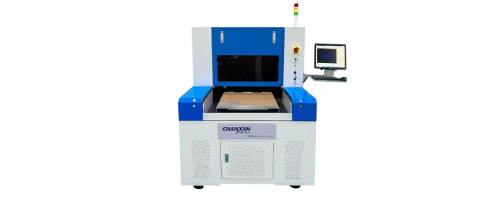
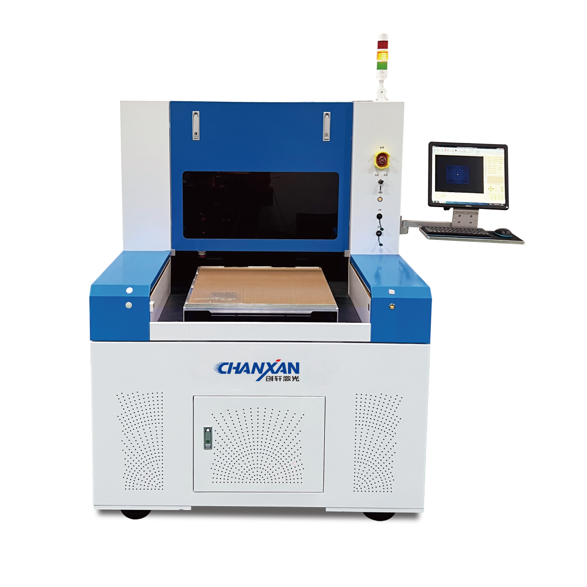
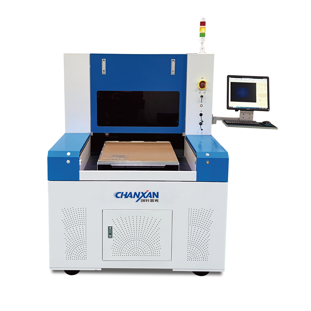
Chanxan ultrafast laser dicing systems utilize advanced picosecond and femtosecond laser technologies to deliver high-yield wafer singulation with zero mechanical stress and minimal thermal impact. Engineered for high-stakes B2B semiconductor lines, our systems are optimized for challenging compound semiconductors (including SiC and GaN), high-precision silicon wafers, glass substrates, and advanced ceramic packages.
Whether you need to eliminate HAZ, shrink your dicing streets, or transition away from high-maintenance mechanical blades, we design turnkey solutions tailored to your cleanroom specifications.
Ready to upgrade your semiconductor wafer processing yield and precision?
Contact Chanxan to Get a Quotation| Free solution
Previous: Laser Processing of Coverlay for Flexible Printed Circuits: A Technical Overview
Next: Semiconductor Laser Dicing: Laser Ablation vs Stealth Dicing Guide