Key Words: Silicon Wafer Dicing PCB Depaneling Glass Cutting
Home > News > Industry News
【Description】:
Discover how UV laser drilling achieves sub-50 micron precision in HDI FPC manufacturing. Eliminate HAZ & boost yields with Chanxan's ultrafast system.
Technical Insights, Market Benefits, and Ultrafast Solutions for High-Density Flexible Electronics
The relentless drive toward miniaturization, lighter form factors, and high-frequency data transmission in consumer electronics, automotive sensor grids, and medical diagnostics has pushed High-Density Interconnect (HDI) Flexible Printed Circuits (FPCs) to their physical limits. In modern FPC fabrication, routing a massive matrix of electrical signals through tight geometries requires robust microvia structures. Achieving consistent, defect-free microvias with diameters spanning < 50 um is no longer feasible with traditional mechanical methods. Instead, high-precision FPC laser drilling has emerged as the global industry standard to achieve reliable sub-50-micron precision.
Flexible Printed Circuits typically comprise alternating layers of polyimide (PI) dielectric films, acrylic or epoxy adhesives, and ductile rolled-annealed (RA) or electrodeposited (ED) copper foils. Processing this heterogeneous stackup presents significant material challenges, as each layer possesses wildly disparate thermal thresholds, mechanical stiffnesses, and optical absorption characteristics.
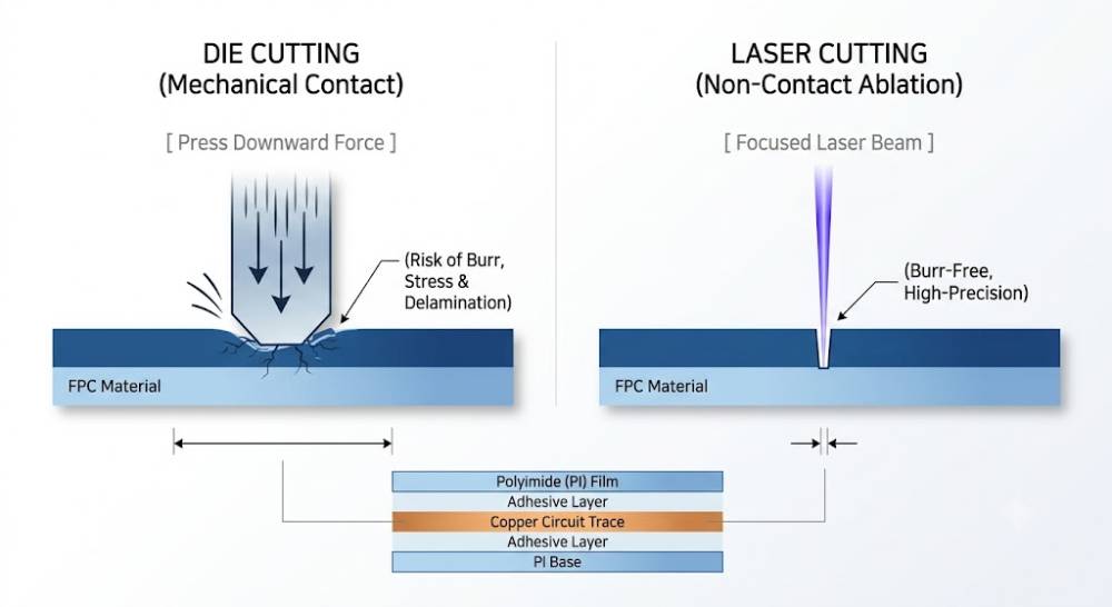
Traditional mechanical drilling relies on physical CNC drill bits. As target via diameters shrink below 100 microns, mechanical bits suffer from extreme fragility, leading to high breakage rates, severe tool wear, and steep operational costs. More critically, mechanical force exerts severe downward shear stress on the flexible substrate, causing inner-layer delamination, copper burrs, and material deformation around the via wall.
The Physics of UV Precision & Cold Processing
Advanced microvia laser drilling circumvents mechanical drawbacks by replacing physical contact with localized electromagnetic radiation. Ultraviolet (UV) light operates at short wavelengths (typically λ = 355 nm). Unlike longer wavelength infrared (IR) or CO2 lasers (λ = 10.6 μm) which ablate materials via thermal vaporization, UV lasers operate primarily via photo-ablation. The high-energy photons of a 355 nm UV beam directly disrupt the molecular covalent bonds within the polyimide matrix, cleanly ejecting the material as microscopic debris with minimal thermal diffusion.
Transitioning to specialized UV ultrafast laser systems directly addresses the most pressing quality bottlenecks in high-density flexible circuit board fabrication:
Elimination of the Heat-Affected Zone (HAZ): Because UV photo-ablation minimizes localized heating, the peripheral thermal degradation zone is exceptionally tight. Maintaining a heat-affected zone HAZ < 3 um prevents the polyimide film from shrinking, melting, or warping, ensuring structural integrity in high-density pad patterns.
Exquisite Depth Control and Blind Via Accuracy: Multi-layer FPCs demand precise blind via drilling, where a microvia must penetrate the top polyimide layer and stop exactly on an inner copper target pad without burning through it. UV lasers can be carefully calibrated to leverage the high ablation threshold of copper relative to polyimide, operating as a self-limiting stop-layer process.
Burr-Free and Smear-Free Profiles: Mechanical drilling and thermal CO2 processing frequently leave epoxy resin smears or copper burrs along the via walls, which jeopardize the continuity of subsequent electroplating steps. Precision UV drilling produces vertically perpendicular, smooth via sidewalls completely free of carbonized residue.
Adopting advanced UV laser processing systems directly translates into structural financial and competitive advantages for manufacturers seeking higher production yields and industrial scalability:
| Operational Metric | Traditional Processing | Advanced UV Laser Systems | Business Value Delivered |
|---|---|---|---|
| Via Diameter Limit | > 75 um (High Defect Rate) | Sub-50 um Down to 20 um | Unlocks next-gen HDI and 5G/6G smartphone circuit contracts. |
| Consumable Costs | High (Frequent drill bit breakage) | Zero (Non-contact tool) | Drastically reduces ongoing Opex and machine downtime. |
| Yield Rates | Variable due to mechanical stress | Consistent > 99.5% Precision | Minimizes material waste, scraping costs, and QA bottlenecks. |
| Tooling Flexibility | Fixed tool geometries | Software-driven patterns | Instant proto-to-production shifts with zero tooling changeover. |
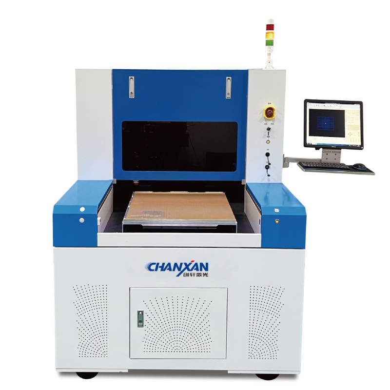
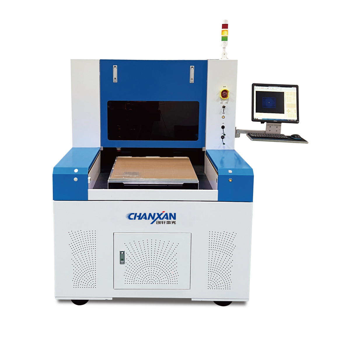
To meet the stringent manufacturing mandates of Tier-1 technology sectors, Chanxan Laser has engineered an industrial-grade flagship solution: the Chanxan UV Picosecond Laser Micromachining System.
While standard nanosecond UV lasers are highly capable, their pulse widths still allow brief thermal conduction into surrounding substrates. Chanxan Laser elevates processing capabilities by compressing the laser pulse width into the picosecond domain (10-12 seconds). This ultra-short pulse duration acts faster than the thermal relaxation time of copper and polyimide. The material transitions instantly from a solid to a plasma state before heat has a chance to propagate through the molecular lattice, offering a premium solution for both high-end FPC laser cutting and blind via processing.
Near-Zero Thermal Impact (HAZ < 3um): Provides immaculate microvia edge quality with absolute zero carbonization, discoloration, or melting, eliminating post-process chemical desmearing stages entirely.
Sub-50 Micron Engineering: Integrated with high-resolution, high-speed digital galvo-scanners and real-time vision alignment systems, the platform effortlessly drills repeatable 20 um to 50 um blind and through-vias across large-format FPC sheets.
Multi-Material Versatility: Perfectly optimized for high-frequency low-loss materials, including Modified Polyimide (MPI), Liquid Crystal Polymer (LCP), and ultra-thin flexible copper clad laminates (FCCL).
Industrial-Grade High Throughput: Built upon a high-rigidity marble granite stable platform and equipped with linear motor drives, Chanxan’s platform delivers 24/7 continuous production reliability with maximum positional accuracy.
As Western markets scale up advanced automotive ADAS, IoT hardware, and aerospace instrumentation, upgrading your manufacturing asset base to high precision is a prerequisite for compliance. Chanxan Laser provides comprehensive global technical support, customer application training, and Free Sample Testing Services. Send your FPC substrates to our laboratory, and let our application engineers demonstrate our sub-50 micron precision profiling capabilities on your proprietary materials.
Contact our engineering desk today for a tailored quotation: wmb@chanxan.com
| Free solution
Previous: Picosecond Laser Cutting for Flexible PCBs: Minimizing HAZ and Carbonization
Next: Flexible PCB Manufacturing Process: Structure, Materials and Laser Processing