

Key Words: Silicon Wafer Dicing PCB Depaneling Glass Cutting
Home > News > Industry News
【Description】:
An in-depth guide to micron-level glass cutting, covering precision requirements, laser technologies, compatible materials, applications, limitations, future trends, and Chanxan Laser solutions.
The demand for micron‑level glass cutting has surged across multiple industries—from consumer electronics and display manufacturing to medical devices, semiconductor packaging, and optical engineering. As devices become smaller, thinner, and more complex, the need for cutting glass with micron‑scale precision, crack‑free edges, and minimal material damage has become a critical manufacturing requirement.
Glass is fundamentally difficult to machine. It is hard, brittle, and transparent—properties that make traditional mechanical cutting methods problematic. Chipping, micro‑cracks, and subsurface damage are common defects that significantly reduce component strength and optical performance. Even thermal laser methods, such as CO₂ cutting, often introduce heat‑affected zones that compromise material integrity.
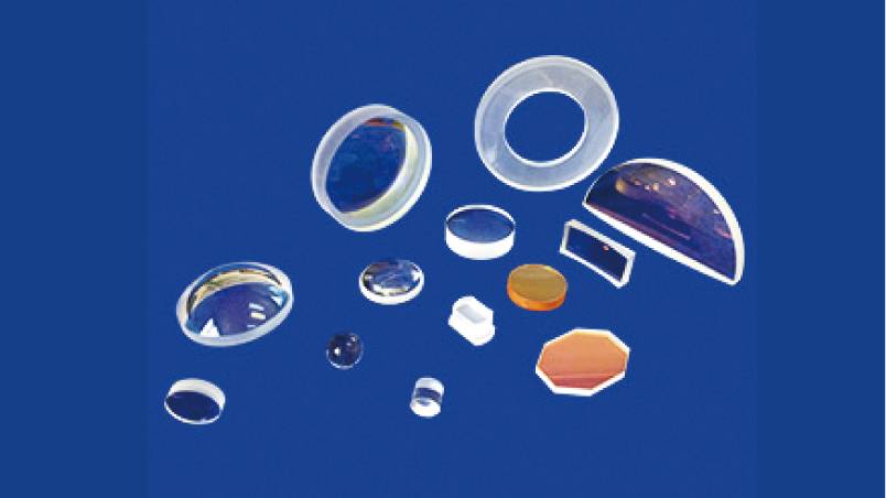
Micron‑level glass cutting refers to the ability to cut glass with dimensional accuracy and edge quality measured in micrometres (µm). This level of precision involves achieving:
Why micron‑level precision matters:
In applications such as foldable displays, medical microfluidics, and semiconductor packaging, even micro‑scale defects can cause catastrophic failure. A 10 µm chip at the edge of a UTG cover glass can propagate under folding stress, reducing fold endurance from >200,000 cycles to <50,000 cycles. A 20 µm deviation in a microfluidic channel can disrupt fluid flow and compromise diagnostic accuracy. In optical systems, edge roughness scatters light and degrades performance.
Several technologies are capable of achieving micron‑level precision in glass cutting:
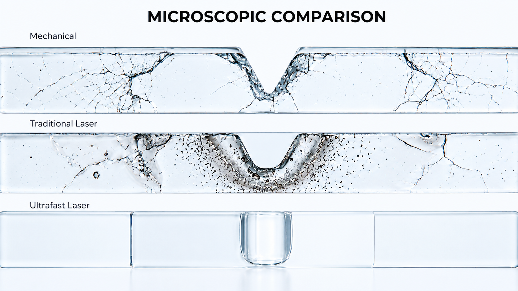
The transition from mechanical to laser‑based glass cutting represents a paradigm shift in manufacturing capability. Among the various laser technologies available, each offers distinct advantages and limitations that make them suitable for specific applications. Understanding these differences is essential for selecting the right solution for a given manufacturing requirement.
UV nanosecond lasers operate at a wavelength of 355 nm, which is strongly absorbed by glass. This absorption enables efficient material removal through a combination of photochemical and photothermal mechanisms. However, because the pulse duration is in the nanosecond range—typically 10 to 50 nanoseconds—there is sufficient time for heat to diffuse into the surrounding material during each pulse.
How it works: The UV laser energy heats the glass surface, causing localised melting and vaporisation. Each pulse removes a small amount of material, and multiple passes are used to achieve the desired depth. The process is essentially thermal in nature, though the UV wavelength reduces the thermal load compared to IR lasers.
Characteristics: UV nanosecond cutting produces acceptable edge quality for many applications, with smooth surfaces that are generally free from gross defects. However, the thermal component of the process means that a small heat‑affected zone is inevitable. This can create residual stress in the glass, which may not be immediately visible but can affect long‑term reliability. For most thin glass applications, the edge quality is sufficient without requiring additional processing.
Limitations: As glass thickness increases, the thermal effects become more pronounced. The heat‑affected zone grows larger, and the risk of micro‑crack formation increases. Additionally, the processing speed is moderate because the material removal rate per pass is limited by thermal diffusion.
Best suited for: Thin glass cutting (<1 mm), cover glass, display panels, and general precision cutting where edge quality requirements are moderate and high throughput is not the primary concern. It is a cost‑effective entry point into laser glass cutting.
UV picosecond laser technology represents the current industry standard for high‑precision glass cutting. The combination of 355 nm wavelength with ultra‑short pulse duration—typically less than 10 picoseconds—enables a fundamentally different material removal mechanism: cold ablation.
How it works: The picosecond pulse deposits energy so rapidly that it is absorbed before heat has time to diffuse away from the focal spot. The material at the focus is converted directly from solid to plasma, bypassing the melt phase entirely. This process removes material with virtually no thermal impact on the surrounding glass. The heat‑affected zone is so small that it is effectively negligible for most practical purposes.
Characteristics: UV picosecond cutting produces edges of exceptional quality. The cutting surfaces are smooth, with no evidence of melting, charring, or thermal stress. Micro‑cracks are eliminated because there is no thermal shock and no mechanical force. The edge strength approaches that of the bulk material because the glass structure is preserved.
What makes it the gold standard: The cold ablation mechanism is particularly important for chemically strengthened glasses, such as aluminosilicate cover glass. These materials have a compressive surface layer that provides their strength. Any thermal input weakens this layer, reducing edge strength and making the glass susceptible to fracture. UV ps cutting preserves the compressive layer intact, maintaining the full strength of the material.
Versatility: Beyond cutting, UV ps lasers are capable of drilling, slotting, and micro‑structuring glass with the same micron‑level precision. Through‑glass via drilling for semiconductor packaging is one notable example where the technology excels, achieving high aspect ratios with smooth, vertical sidewalls.
Best suited for: The most demanding applications, including UTG for foldable displays, chemically strengthened cover glass, OLED panel glass, optical components, TGV drilling, and any application where edge quality and material integrity are critical.
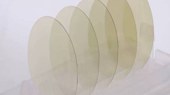
Femtosecond lasers operate with pulse durations below 500 femtoseconds—three orders of magnitude shorter than picosecond lasers. This extreme pulse duration pushes the cold ablation mechanism to its ultimate limit.
How it works: The energy is deposited so rapidly that the material at the focal point is effectively removed before any physical or thermal effects can propagate. The process is purely photomechanical, with zero thermal diffusion.
Characteristics: Femtosecond cutting delivers the highest possible edge quality. The surfaces are ultra‑smooth, with no measurable heat‑affected zone. The edges are pristine, preserving the glass's optical and mechanical properties to the greatest extent possible.
Limitations: The technology comes with significant trade‑offs. Femtosecond lasers typically have lower average power than picosecond systems, making them slower for production applications. The equipment is also more expensive to purchase and maintain. These factors limit the technology primarily to research and development, and to highly specialised production applications where throughput is not the primary constraint.
Best suited for: R&D, ultra‑high‑precision optics, internal 3D structuring, waveguide fabrication, and exotic materials where ultimate edge quality is required and throughput is less critical.
Filamentation cutting represents a fundamentally different approach to glass processing. Instead of ablating material from the surface, the laser is focused inside the glass volume.
How it works: The high peak power of a picosecond or femtosecond laser induces a phenomenon called filamentation. The beam propagates through the transparent material, creating a stable filament of modified glass. This filament is a region where the glass structure has been altered—density changes, micro‑voids, or refractive index variations. The filament extends through the thickness of the glass, forming a precise internal guide path.
Separation: After the filament is formed, the glass is separated along this modified path. Separation can be achieved through several methods: mechanical bending, thermal stress (using a CO₂ laser), or chemical etching. The filament acts as a controlled fracture line, enabling clean separation with minimal edge roughness.
Characteristics: Filamentation cutting produces exceptionally smooth edges because the separation follows the precise internal modification path. The kerf width is extremely narrow—minimising material waste. The process can handle glass from 30 µm up to several millimetres thick. Complex curves and internal contours are achievable because the cutting path is software‑defined.
Applications: Filamentation is particularly valuable for thick glass cutting where pure ablation would be too slow. It is also used for curved profiles and irregular shapes. The technology is becoming increasingly important for display glass, automotive glass, and semiconductor applications.
The choice of cutting technology depends heavily on the specific glass material:
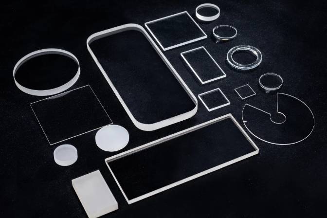
Micron‑level glass cutting is essential across multiple industries where precision, edge quality, and material integrity are critical. The following highlights the key applications and the specific requirements that drive technology selection.
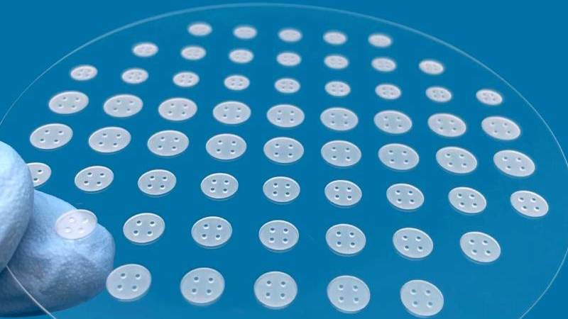
Chanxan Laser offers a comprehensive range of systems designed for micron‑level glass cutting across multiple industries:
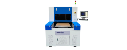
Chanxan systems are proven on a wide range of glass materials: UTG, aluminosilicate (Gorilla Glass), borosilicate, soda‑lime, quartz, OLED display glass, optical glass, sapphire, and more.
Chanxan Laser provides the production‑ready solutions that make micron‑level glass cutting possible. With deep process expertise, advanced system engineering, and a global support network, Chanxan is a trusted partner for manufacturers worldwide.
Share your glass material, thickness, drawings, and precision requirements. Chanxan Laser can help configure a suitable laser processing solution for your application.
Contact to Get a Quote| Free solution
Previous: What Makes Micron‑Level Glass Cutting So Difficult?
Next: How 3D Five-Axis Laser Cutting Machines Process Complex Plastic and Automotive Parts








